 Hello fellows, I hope you all are doing great. In today’s tutorial, we will have a look at Introduction to Schottky Diode. The diode is such an electronic component that used to transform AC into DC with some filter circuits for removal of ripples. The Schottky diode was invented by the physicist H.Schottky who belongs to Germany so it called Schottky diode. It created with the combination of metal and semiconductor material. Its forward biased voltage loss is very less and switching of this diode is also fast. In previous years crystal detectors used in radio receivers were operated as Schottky diodes.
If forward biasing conditions is provided to diodes either silicon diode or Schottky diode current flows through them. The value of forward-biased voltage for silicon diode is almost six hundred to seven hundred millivolts, for the Schottky diode voltage range is forward is one fifty to four-fifty millivolts. Due to less forward-biased voltages switching speed of Schottky is high also increases the efficiency of the circuitry in which it is used. In today’s post, we will have a detailed look at its working, applications, construction, and some related parameters. So let’s get started with Introduction to Schottky Diode.
Introduction to Schottky Diode
- The Schottky diodes are also called hot-carrier diodes, or Schottky barrier diode used in such applications where large frequency and high-speed switching speed is required.
- It called a hot-carrier diode due to the high energy level of electrons in N part than the metallic portion of a diode.
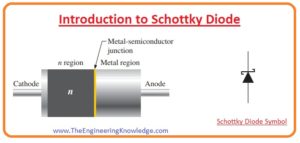
- The symbol of a diode is shown in the below figure. For the construction of this diode semiconductor material normally doped with the N, the material is combined with metals such as silver, gold, or platinum.
- In this diode, there is no PN junction like other diodes but it has a semiconductor to a metal junction.
- The forward-biased voltage loss for this diode is normally 0.3 volts due to the absence of depletion in this diode.
- The current flow of this diode is due to majority charge carriers and there is no minority charge carriers that exists in this diode and also no reverse leakage current flow.
- The metallic part of this diode is completely covered with the conduction band electrons and n region of this diode is less doped.
- When a diode is in forward biasing conditions then high energy electrons existing in N part move to the metallic part and loss their energy in this region.
- Due to the absence of minority charge carriers in this diode biasing changes fast.
- This diode is used in higher frequency and switching applications such as in digital circuitry.
Schottky Diode Construction
- In the Schottky diode, the metal-semiconductor junction is created among metallic material and semiconductor that called Schottky barrier.
- In the construction of this diode gold, platinum, tungsten and some silicides are used with the semiconductor material that is N-doped.
- The metallic part of this diode functions as an anode and N part is a cathode which means current can move from metallic part to the semiconductor according to the conventional direction of the current.
- The Schottky barrier of this diode sources the high-speed switching and less loss of forward-biased voltage.
- The forward voltage required for a diode depends on the metal and semiconductor material used. Both N and P-type semiconductor material can be used to make Schottky barrier but forward biased voltage for P-type material is less.
- With the decrement in forward biased voltage reverse leakage current increases that so voltage value for P-type material is kept in the range of 0.5 to 0.7 volts.
Schottky Barrier
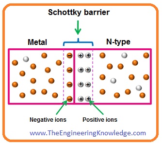
- A Schottky barrier is created at the meeting point of metal and N-type semiconductor material.
- It is also called the potential energy barrier created at the metallic semiconductor junction.
- Electrons cross this energy barrier to move about the diode.
- The rectifying Metal-semiconductor connection creates a rectifying Schottky barrier.
- This rectifying Schottky barrier is used for creating an expedient recognized as a Schottky diode.
- The non-rectifying metallic-semiconductor connection makes a non-rectifying Schottky barrier.
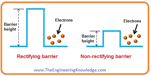
- The main feature of the Schottky barrier is the height of this barrier. This height depends on the mixture of semiconductor and metal.
- The non-rectifying barrier has less height of the Schottky barrier while the height of the Schottky barrier of the rectifier barrier is high.
- The barrier high for non-rectifier Schottky barrier is less so the depletion region can not create the depletion region. So in this region, the depletion region is not present.
- While in rectifying the Schottky barrier the hight of a barrier is high so the depletion region exits.
- If metallic material is connected with the less doped semiconductor material than rectifying Schottky barrier is created.
- While if highly doped semiconductor material is connected with the metal than a non-rectifying barrier is created.
Schottky Diode Energy Band
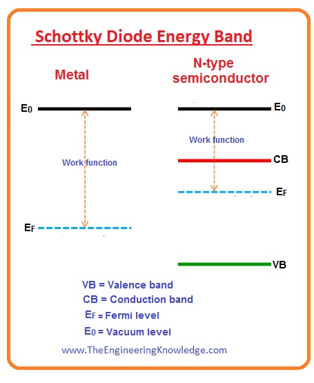
- In the below figure energy band diagram for N-type semiconductor material and metallic material is shown below.
- The energy level of electrons at the outer side of the substance is known as the vacuum level.
- The energy required to move an electron from Fermi level (EF) to vacuum level (E0) is called work function.
- The value of work function is different for metallic and semiconductor materials. The work function needed for the metallic material is larger than the semiconductor material.
- So potential energy for electrons in N-type semiconductor material is large than the electrons of metallic substance.
- The potential energy of electrons at high energy level is high than the electrons in the less level of energy.
- Due to this energy of electrons in N types, a semiconductor material is larger than the electrons in metallic materials.
- The energy band figure of metallic material and N-type material after the combination is in the below picture.
- With the combination of N material with metallic substance, the resultant component created known as Schottky diode.
V-I Characteristics of Schottky Diode
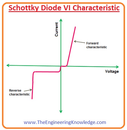
- In the below figure the voltage-current characteristics is shown.
- The line at the Y-axis defines the current flowing through the diode and X-axis voltage provided to the Schottky diode.
- You can see that the characteristic curve of the Schottky diode is similar to the normal diode with the difference is that forward biased voltage for Schottky diode is less than the general diode.
- The voltage drop for forward-biased Schottky diode is 0.2 to 0.3 volts while for a silicon diode is 0.6 to 0.7V.
- The reverse saturation current for Schottky diode is less than the normal diode.
Difference between Schottky and PN Junction Diode
- These are some differences between Schottky and PN junction diode.
| Schottky Diode | PN Junction Diode |
| In this diode current flows due to the electrons but very less due to minority holes. | In this diode current flows due to both electrons and holes. |
| Schottky diode is known as a unipolar device due to electron current. | It known as bipolar as in this diode current flows due to electrons and holes. |
| The reverse breakdown voltage of the Schottky diode is less than the normal diode. | Its reverse breakdown voltage is high than the Schottky diode. |
| There is no or less depletion region in this diode. | It has a depletion region. |
| Its turn-on voltage is less than a normal diode. | Its turn-on voltage is high. |
| For Schottky diode, electrons are majority charge carriers in both metallic and semiconductor regions. | In this diode, electrons are majority carriers in the N region and minority carriers in the P region. |
Schottky Diode Limitations
- These are some limitations of the Schottky diode.
- The most common limitation of the Schottky diode is less reverse voltage rating large reverse leakage current.
- Normally reverse voltage for Schottky diode is fifty volts or less than fifty.
- Some diode for the value of voltage larger than two hundred is also available.
- The increment in reverse leakage current flow increases the heat of diode. That decreases the suitable reverse voltage to less than the real rating of the diode.
- Whereas large reverse voltages are attainable, they would exist a larger forward voltage, analogous to other types of typical diodes.
Silicon Carbide Schottky Diode
- The Schottky diodes manufactured with silicon carbide have less value of reverse leakage current compared to Schottky diode constructed with the silicon.
- With less reverse current has a large value of forward biased voltage almost 1.4 volts to 1.8 volts at twenty-five degrees Celsius and reverse voltage also large.
Schottky Diode Applications
- These are some applications of Schottky diode.
Voltage Clamping
- The forward voltage loss for silicon diode is almost 0.6 volts and for the germanium diode is 0.2 volts while the forward voltage loss for Schottky diode is from 0.15 volts to 0.46 volts due to this it used in clamping circuits.
Switched-Mode Power Supply
- The switch-mode power supply used Schottky diodes for the rectification process. The less forward voltage and fast recovery time enhance efficiency.
Reverse Current and Discharge Protection
- As less forward voltage loss for the Schottky diode due to that small power is dissipated as heat so it is preferred for such applications where high efficiency is required.
- For example, photovoltaic systems to stop the discharging of batteries used with the solar panels, these diodes called blocking diodes.
- These diodes used in a grid-connected network having numerous strings associated in parallel, to stop the reverse current passing from neighboring strings through shaded strings.
Related Posts
- Current Regulator Diode
- Zener Diode
- Step Recovery Diode
- PIN Diode
- Schottky Diode
- Photodiode
- Varactor Diode
- Diode
- Zener diode Applications
- Laser Diode
- LED
So friends that is complete post about Schottky diode if you have any further query about Schottky diode ask in comments. See you in the next post. Have a good day. Thanks for reading.


Amazing post. Articles which have meaningful and insightful remarks are more enjoyable, at least to me.
It’s interesting to read what others thought and how it relates to them or their clients, as their perspective could possibly help you later on.
King regards,
Thomassen Henneberg
I like what you guys are up too. Such clever work and reporting! Carry on the superb works guys I have incorporated you guys to my blogroll. I think it’ll improve the value of my website 🙂
I was suggested this blog by my cousin. I am not sure whether this post is written by him as no one else know such detailed about my problem.
You’re incredible! Thanks!