 Hello, readers welcome to the new post. In this post, we will discuss Introduction to 75160B. It is SN75160B eight-channel general-purpose interface bus or GPIB transceiver. That is a monolithic high-speed low power power-consuming Schottky component that is configured to transmit the data in two-way communication through a single point transmission line.
Its feature is such that can be functioned in passive pullup or three-state mode. In this post, we will discuss its working, features, and some other parameters. So let’s get started. Introduction to 75160B.
Introduction to 75160B
- The 75160B is a transceiver that is designed according to IEEE standards 488 to 1978. Its output is configured in passive pullup or three-state output mode through PE in the high state.
- It talks enable or TE is in a high state these ports provide the feature of passive-pullup outputs when pullup enable PE is low and three-state output if PE is the high state.
- Getting TE low mode these ports are in a high impedance state. Driver outputs are configured to handle loads up to forty-eight milliamperes of sink current.
- Output glitches through power up and power down are removed through inner circuitry which disables both bus and receiver outputs.
- The output does not load the bus if Vcc=0. If there is the configuration of the SN7516B bus transceiver pair offers the complete sixteen-wire interfacing for the IEEE-488 bus.
- The structure of SN75160B is featured from zero to seventy centigrade.
75160B Features
- Its main features are explained here
- It is compatible with the IEEE Standard 488 to 1978 GPIB
- It is eight channel bidirectional transceiver
- It is a high-speed device, uses less power, and has Schottky circuitry configured device
- It has less power dissipation about seventy milliwatts for one channel
- Its propagation time is about 22ns maximum
- It has high impedance PNP configured inputs.
- Receiver hysterics is about 650mV TYP
- Its structure is open collector drive output point
- It is no loading of nus for Vcc=0
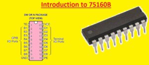
75160 Pinout
- 75160 Pin are explained here
| Pin No | Pin Name | Pin Function |
| 01 | TE | It is Talk Enable Pinout |
| 02 | B1 | It is GPIO or General purpose interface input/output pin B1 |
| 03 | B2 | It is GPIO or General purpose interface input/output pin B2 |
| 04 | B3 | It is GPIO or General purpose interface input/output pin B3 |
| 05 | B4 | It is GPIO or General purpose interface input/output pin B4 |
| 06 | B5 | It is GPIO or General purpose interface input/output pin B5 |
| 07 | B6 | It is GPIO or General purpose interface input/output pin B6 |
| 08 | B7 | It is GPIO or General purpose interface input/output pin B7 |
| 09 | B8 | It is GPIO or General purpose interface input/output pin B8 |
| 10 | GND | It is the ground pin and ground attached here |
| 11 | PE | It is the Pullup Enable terminal |
| 12 | D8 | It is Input Output Pin D8 |
| 13 | D7 | It is Input Output Pin D7 |
| 14 | D6 | It is Input Output Pin D6 |
| 15 | D5 | It is Input Output Pin D5 |
| 16 | D4 | It is Input Output Pin D4 |
| 17 | D3 | It is Input Output Pin D3 |
| 18 | D2 | It is Input Output Pin D2 |
| 19 | D1 | It is Input Output Pin D1 |
| 20 | VCC | Here positive power is provided |

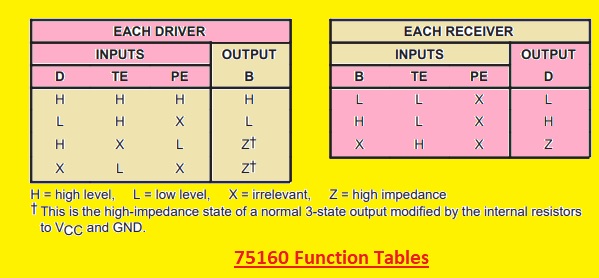
75160 Function Tables
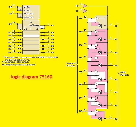
logic diagram 75160
Read also
- Introduction to SN75176BP Bus Transceiver
- What are Integrated Circuits | Types, Uses, & Function
- Introduction to SP3485, Features, Pins, & Working
- Introduction to Mobile Network or Cellular Network Management System
That is all about the 75160B all details has explained about this transceiver. If you have any query ask here thanks for reading have a nice day.