
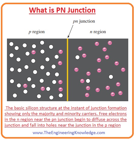
Hello, friends, I hope all of you are having fun in your life. In today’s tutorial, we will explain what a PN junction is. The PN junction is a line between 2 different categories of semiconductors; it forms when we dope any semiconductor material with a doping element. If we doped any silicon crystal with a pentavalent impurity and other parts of the silicon atom with a trivalent impurity, then the boundary between these parts is called a PN junction.
The portion of silicon doped with the pentavalent impurity has electrons as majority charge carriers, and the part of silicon with a trivalent impurity has holes as majority charge carriers. In today’s post, we will have a look at its formation, applications in different electronic devices, and some other related parameters. So let’s get started with what a PN junction is.
What is a PN junction?
A PN junction is the partition between two different semiconductor materials when a single material is doped with 2 different materials.
Any p-type substance has 2 main materials. The first one is pure, like silicon, that is doped with the trivalent impurity such as boron.
Due to the addition of boron, silicon holes are created in the silicon structure. But due to the equal amount of protons and electrons in a complete substance, the total charge is ‘0’ on the substance.
Similarly, in an N-type silicon substance, pentavalent impurity is doped, and free electrons are available in the structure.
But due to an equal amount of protons and electrons, the net charge on this substance is still zero.
If pure silicone material is doped with N impurity as well as with the P impurity, then the partition between them is known as a PN junction; it is shown in the given figure.
In the p portion, there are numerous holes as majority carriers, and in the n portion, electrons are the majority carriers.
Formation of the Depletion Region
When a PN junction has formed, the electrons in the n portion of the PN junction move in any direction and collide with other atoms and electrons.
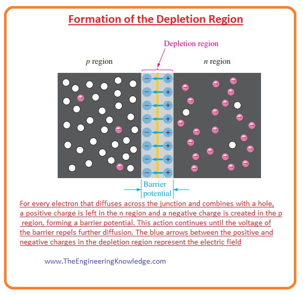
The electrons close to the junction and high energy move to the P portion and merge with the hole shown in a given figure.
As above, we discuss when there is no pn junction created; then there are the same number of electrons and protons in the N-type substance and the total charge is zero.
This condition is also the same in P-type materials.
After the creation of a junction, the free electrons in the n portion cross the junction, creating a positive ion on the n side and a negative ion created due to the combination of electrons and holes.
On the ‘n’ side, due to electrons, a positive ion layer is produced, and on the ‘P’ side, a negative ion layer is generated due to these 2 layers of the ion depletion region being created.
As you can see, the area of the depletion region is less than that of the ‘N’ and ‘P’ regions.
After a certain time interval, movement of electrons from the ‘N’ to the ‘P’ side stops, and equilibrium is created.
Further movement of electrons and holes is repelled by the depletion region as its area also increases, and positive ions in the ‘N’ region repel holes and negative ions in the ‘P’ region repel electrons, and it behaves like a barrier.
Potential Barrier
- As we are familiar with the Coulomb force, any positive charge or negative charge has it’s on the electric field.
- In the depletion region, there is numerous positive and negative charge that forms an electric field. This field is created due to the force of attraction among opposite charges.
- This electric field is shown in the given below by the blue lines. This field is a barrier for free electrons in n regions to move to the P side.
- It means there is a need of some external energy for an electron to cross this barrier.
- The potential difference across the depletion region is the number of volts needed for electrons to cross this field.
- This potential difference is known as a potential barrier and is measured in volts.
- Some factors define the potential barrier and the required voltage for it.
- Type of semiconductor material.
- Temperature
- Doping
- The potential barrier voltage for germanium is 0.3 volts and for silicon is 0.7 volts.
Energy Diagrams of the PN Junction and Depletion Region
In ‘N’-type substances, the valence and conduction bands are at a lower energy level than the P-type valence and conduction bands.
As we discussed above in ‘P’ materials, impurities from group three of the periodic table, or trivalent impurities, are doped, and in ‘N’ substances, pentavalent impurities are added.
The force applied by the trivalent impurities on valence shell electrons is less than that of pentavalent impurities.
The less force exerted in P-type substances indicates the orbits in which electrons are moving are at a larger distance from the center and have a higher value of energy than the electrons’ orbits of N-type substances.
The energy diagram at the start of PN junction creation is drawn in the figure below.
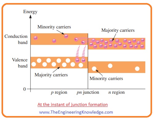
- In this figure, you can see that the valence and conduction bands in n parts are at less energy level while P is at a high energy level.
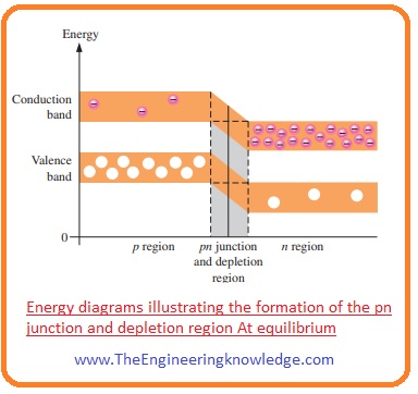
The electrons in the N part that exits at the upper portion of the conduction band can cross the potential barrier very easily.
After leaving N, the electron loses its energy and combines the hole in the P portion; you can see it in the above-given figure.
The movement of electrons that have high energy continues to the P side of the substance, and a depletion region is created.
After that, fewer high-energy electrons of high energy value are in the n region or no electrons in the conduction band of the N part; these arrangements are shown in the figure given below.
At this point, the PN junction is in an equilibrium state, and the depletion region has been created or finished due to the stoppage of the electron movement.
Read also
- Difference between PN Junction Diode and Schottky diode
- Difference Between PN Junction & Zener Diode
- Introduction to PN2222, Working, Pinout, Features
- Introduction to S8050 – NPN Transistor
- Introduction to 2N2907 PNP Transistor
That is the detailed post on the PN junction I have mentioned each and every parameter related to this junction with the detailed. If you have any query and want to add something more in this post share in the comments box. Thanks for reading. See you in the next tutorial.



I needed to thank you for this very good read!! I certainly loved every bit of it. I’ve got you bookmarked to check out new things you post…
It composed his thoughts while reading the article amazingly
King regards,
Balle Hessellund
Thank you for your entire efforts on this blog. Betty take interest in doing internet research and it’s easy to understand why. Most people know all relating to the lively way you render very useful ideas by means of the blog and as well welcome response from other people about this article so our daughter is truly learning a lot of things. Take advantage of the remaining portion of the year. You have been carrying out a powerful job.