 Hello fellows, I hope you are doing great. In today’s tutorial, we will have a look at Introduction to Zener Diode. The diode is a semiconductor device that used to convert AC current into DC current. In general diode current flows in only forward biasing condition and block the flow of current in reverse biasing conditions. In forward biasing the resistance offered by the diode is less and in reverse biasing resistance offered by the diode is high. If we increase the voltage across the diode in reverse biasing condition then one point comes where the current starts to flow in reverse biasing condition. At this point with the less variation in voltage, there is a large amount of current increment in reverse biasing mode.
The abrupt increment in the current is called avalanche breakdown or Zener breakdown. The voltage at which this Zener avalanche exit is called Zener voltage and current is known as Zener current. The general diode can not operate in a breakdown region as in this region a large amount of current can damage the diode. There is a special diode that can operate in Zener or avalanche breakdown without damaging is known as Zener diode. In forward biasing conditions it operates similarly to the normal diode and a large amount of current flows through it. In today’s post, we will have a detailed look at its working, construction, applications, V-I characteristics, and some other related parameters. So let’s get started with Introduction to Zener Diode.
Introduction to Zener Diode
- The Zener diode is a type of diode that operates in the reverse breakdown region in which a general diode is not operated.
- If the voltage is across anode of the diode is positive and across cathode is negative than it operates in alike to a normal diode.
- If the voltage at anode is negative and a cathode is positive than the value of the reverse voltage at which breakdown occurs and reverse current start to flow is called Zener voltage.
- This process was discovered by Clarence Zener who was American Physicist and known as Zener effect.
- There are different values for different Zener voltages for Zener diodes some diodes have a property to regulate the value of Zener voltage.
- The doping level of the Zener diode PN junction is larger than the normal diode. The reverse breakdown similar to Zener diode also occurs in normal diode but the curve in case of reverse breakdown is not fine in normal diode as in Zener diode.
- Zener diode can operate in a breakdown region but the general diode can not get damage for this region.
- But the design of a Zener diode is such that it can operate very easily in a breakdown region without any disturbance.
- Zener diode is almost used in every electronic instrument and is the main element of any circuitry of devices.
- These diodes are also used to provide protection to any circuitry from overvoltage especially electrostatic discharge (abrupt flow of current among 2 charged objects).
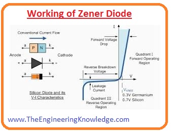
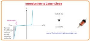
- The symbol of Zener diode is shown in the below figure. In this, figure the operation region of Zener diode also shown.
Zener Breakdown
- The designing of Zener diode is such that it can function in a reverse breakdown. There are 2 types of reverse breakdown in the Zener diode.
- The first one is an avalanche and the second one is Zener breakdown.
- The avalanche breakdown occurs at the high value of reverse voltage.
- While Zener breakdown occurs at less value of reverse biasing voltage.
- For decrement in the value of breakdown, the voltage diode has a high value of doping.
- Due to the high value of doping its depletion region is very thin. As a consequence there is field is generated in the depletion region.
- The intensity of field near the Zener breakdown voltage or (VZ) is such high that it can pull out electrons from their valance band and due these electrons current start to flow.
- The Zener diode that has a breakdown value of voltage less than five volts operates at Zener breakdown.
- But Zener diode that has breakdown voltage greater than fie volts operate in Zener breakdown.
- Diode either operating in the breakdown region or in the avalanche region is called Zener diode.
- The normal breakdown voltage range available in market for Zener diode is one volt to greater than two fifty volts with having one to twenty percent tolerance.
Zener Breakdown Characteristics
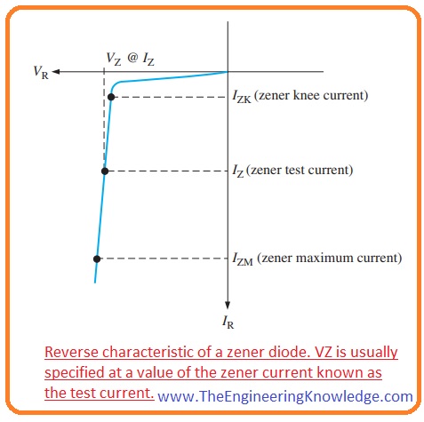
- In below figure characteristic curve for Zener diode in reverse bias is shown.
- You can see that with the increment in reverse voltage VR there is very less increment in reverse current IR to the knee point of the curve.
- This reverse current is also known as Zener current Iz.
- At knee point breakdown effect starts, interior resistance offered by the Zener is called Zener impedance (ZZ) start to decrease with the abrupt increment in the value of reverse current.
- From the lowest point of the knee of curve Zener breakdown voltage (Vz) almost remains constant but very less increment in these voltages due to increment in Zener or reverse current Iz.
Zener Regulation
- The capability of a diode is to maintain the reverse voltage across its terminals constant is the main feature of Zener diode.
- During functioning in the breakdown, region diode operates as voltage regulators since it retains the constant value of voltages across its leads when there is a large increment in the value of reverse current.
- The lowest value of reverse current, IZK, should be sustained for a diode to operate as a voltage regulator in breakdown region.
- In the above figure, you can note that when the reverse current is less than the knee point of a curve, due to that voltage also decrease significantly also diode regulation decreases.
- With the lowest value of current, there is extreme value of current IZM over which diode will damage due to high power dissipation.
- So we concluded that for the reverse current range of IZK to IZM the voltage across Zener diode is constant.
- The nominal voltage VZ for a diode is mentioned on datasheet with the reverse current IR that is known as Zener test current.
Zener Equivalent Circuits
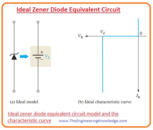
- In the given figure, you can see the ideal Zener diode and its resultant ideal characteristic curve.
- The voltage loss across this diode is constant and equal to the nominal Zener voltage.
- This voltage loss across the diode occurs during the reverse breakdown is denoted by the dc voltage symbol but it is not the property of Zener to generate voltages.
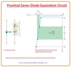
- In the below figure the circuit of a practical diode is shown that has Zener impedance or resistance of diode ZZ.
- As the characteristic curve of this diode is not vertical similar to the ideal diode due to variation in Zener current (ΔIZ) its Zener voltage (ΔVZ) also increases. You can see in the above characteristic curve.
Zz= (ΔVZ)/(ΔIZ)
- Usually, ZZ is stated at the Zener test current. In some conditions, you can suppose that ZZ is a less constant above the complete range of Zener current and it is a purely resistive element.
- It is good to not operate diode close to the knee of the curve since variations in impedance value are high in this region.
- For different circuitry analyses and troubleshooting purposes the ideal diode will provide the best results and it easy to handle than the complex circuitry of a practical diode.
Zener Diode Temperature Coefficient
- The temperature coefficient defines the percent variation in Zener voltage for every degree variation in temperature.
- For instance, due to twelve volts, Zener diode with positive coefficient will show 1.2 millivolts increment in Vz when the temperature of junction enhances on Celsius.
- The given below formula can be used to find variation in Zener voltage resultant to the junction temperature variation for a specific temperature coefficient.
ΔVZ =VZ x TC x ΔT
- In this equation Vz value of nominal Zener voltage at reference temperature 25oC, Tc is the coefficient of temperature and T variation in temperature with respect to the reference temperature.
- The positive Tc indicates that Zener voltage increases with the increment in temperature and decreases with the decrement in temperature.
- The negative value of TC indicates that Zener voltage reduces with the increment in temperature and upsurges with the reduction of temperature.
- In certain conditions temperature coefficient is denoted in mV/°C instead of %/C.
- In these conditions, Vz is denoted as.
ΔVZ=TC x ΔT
Zener Power Dissipation and Derating
- Zener diodes are identified to function at an extreme power named as the maximum dc power dissipation, PD(max).
- For instance, the 1N746 zener rating is PD(max) =500 mW and the 1N3305A rating is PD(max)=50 Watts.
- The formula for dc power dissipation is given here.
PD = VZIZ
Zener Diode Power Derating
- The maximum power dissipation PD(max) of Zener diode is usually defined for a certain value of temperature or over that value such as fifty Celsius.
- Over that specific temperature, the value of PD(max) decreases with respect to the derating factor.
- The derating factor is defined in mW/°C. The maximum derating power can be found by using this below formula.
PD(derated) = PD(max) – (mW/°C)ΔT
Working of Zener Diode
- In normal diode for reverse biasing condition, there is a large amount of current is needed larger than the breakdown voltage.
- When the reverse biasing breakdown voltage is surpassed, then from a normal diode large amount of current flows due to avalanche breakdown.
- This current will continue to flow if it not stopped by any external circuit due to this current heat will produce that will damage the diode.
- The properties of Zener diodes are almost alike to the general diode with the difference is that Zener diode is constructed for the decrement in value of breakdown voltage that is known as Zener voltage.
- With opposite to the normal diode Zener diode in reverse biasing conditions has a control breakdown and has a feature to retain the voltage across the Zener diode near to the Zener breakdown voltage.
- For instance, a diode having a Zener breakdown voltage of 3.2 volts will have a voltage loss of close to 3.2 volts over a different range of reverse current.
- Due to this Zener diode is the best option for such applications where the reference voltage is used such as in amplifiers.
- Another method that generates the same consequence is the avalanche effect such as in avalanche diode.
- There are 2 types of diodes are manufactured in the same technique and have 2 features in this diode.
- The diode constructed with the silicon to the value of 5.6 volts the Zener effect is largest displays a negative temperature coefficient.
- Over 5.6 V the avalanche effect is largest shows a positive temperature coefficient.
Applications of Zener Diode
- These are some applications of Zener diode describe here with the detail.
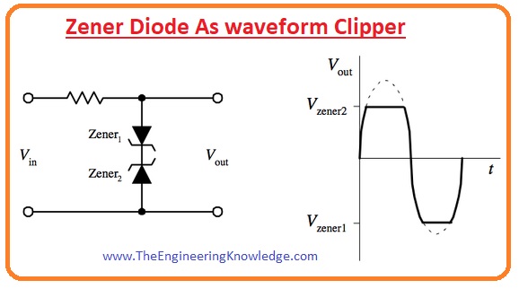
Waveform Clipper
- In the below figure diode as clipper is used in this circuitry 2 diodes are connected series with their faces.
- Due to these arrangements, they will clip both halves of the wave.
- These circuits with the varying the shape of the signal also used to remove the spike in different circuits.
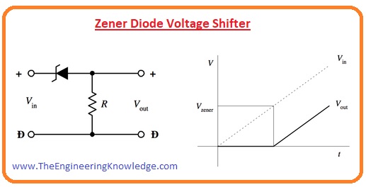
Voltage Shifter
- The Zener diode can also use to shift the voltage.
- This circuitry decreases the output voltage to value equal to Zener diode breakdown voltage. In the below figure circuitry of voltage, the shifter is shown.
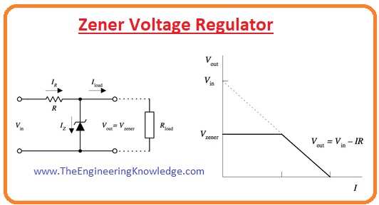
Voltage Regulator
- Zener diode is used in numerous circuits as voltage regulators and provides correspondent value of voltage.
Related Posts
- Current Regulator Diode
- Zener Diode
- Step Recovery Diode
- PIN Diode
- Schottky Diode
- Photodiode
- Varactor Diode
- Diode
- Zener diode Applications
- Laser Diode
- LED
So friends that is complete post about Zener diode I tried my level best to make this post easy and simple for you. If you have any queries about this post ask in comments. See you in next post have a good day. Thanks for reading.


