Hello, fellows, I hope all of you are having fun in your life. In today’s tutorial, we will have a look at the introduction to diodes and their practical implementation. It is an electronic device that has two terminals; the first is positive and the second is negative. A diode allows the current to flow only in a single direction, as it shows a high value of resistance in one direction and less resistance in the other direction. The first diode was created with the crystals of minerals and known as the Cat’s Whisker diode.
There are numerous types of diodes available in the market and used in different electronic projects and devices. The main function of a diode is the conversion of AC current into DC, as some devices require DC for their operation. So a diode is used to operate these devices with the AC at the input terminals. In today’s post, we will have a detailed look at its construction, working, types, and some practical uses in different projects. So let’s get started with the introduction to Diode.
Introduction to Diode
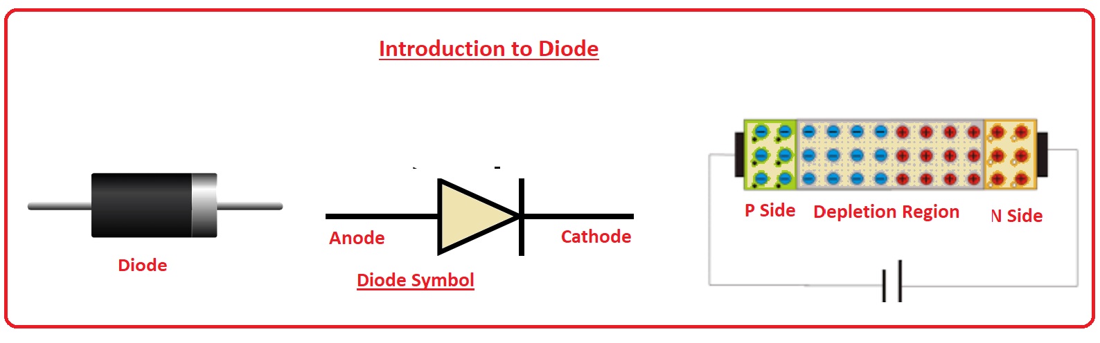
The diode is an electronic component that converts AC into DC by the rectification process and allows current flow only in one direction.
The operation of a diode is similar to the check valve that allows the liquid to flow only in a single direction; similarly, current flows through the diode in only one direction.
The diode is made with the combination of two different semiconductor materials, P and N.
• The P side of the semiconductor is positive and called the anode, and the N side of the diode is negative and called the cathode.
Due to high-temperature tolerance, silicon is used in the construction of diodes, but also germanium is used for diode production when less value of voltage loss is needed.
Typical Diode Packages
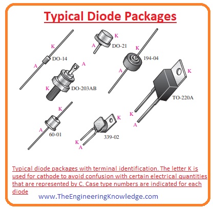
There are numerous packages of diodes available in the given figure; different packages are shown.
The anode and cathode are defined in numerous ways.
Depending on the features, the cathode is defined as a band or tab. In such arrangements of diode structure, it is only when lead exists that the casing of the diode behaves as a cathode.
Surface-Mount Diode
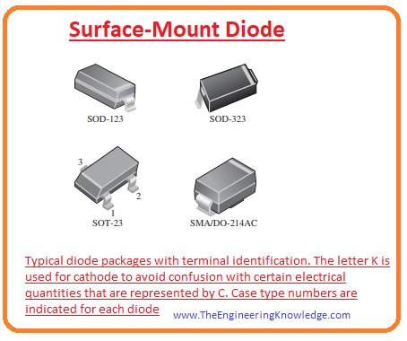
There are numerous diode packages for surface mounting on the PCB board shown in a given figure.
In the figure there are 2 packagings shown: the first one is is SOD (small outline diode) and the second one is SOT (small outline transistor).
The leads in the structure of casing SOT and SOD are like the gull wing.
While in SMA casing, the leads are like the L-shaped ones, which are bent in the casing.
The one point of SOD and SMA is bent and works as a cathode.
Diode Forward Biasing
- Biasing is a process in which an input supply is provided at the terminals of diode.
- In forward-biased condition current flows due to movement of electrons and holes across the PN junction.
- In given figure, you can see that the diode is attached with the dc voltage source in the forward-biased direction.
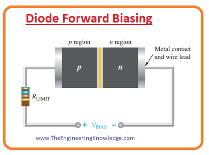
The voltage biased provided by the external DC source is represented as Vbias.
You can see that in the circuit, the resistance is connected in series with the battery and diode; it is for limiting the value of current and is known as current limiting resistance.
There are 2 conditions that should be followed for the forward biased condition.
The first is to connect the anode of a diode with the positive terminal of the battery and the cathode with the negative terminal of the battery.
In the second condition, the value of the voltage source connected with the diode should be larger than the potential barrier.
The behavior of the diode after forward biasing is shown in a given figure
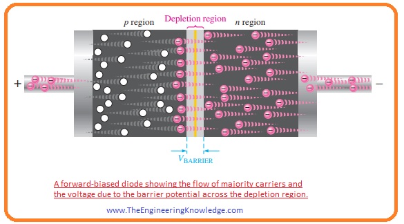
As we know, similar charges oppose each other, so the negative terminal applies force on the electrons in the N region, and they start to move towards the PN junction.
Due to the movement of electrons, current flows through the electrons.
As the negative terminal of the battery continuously provides energy to the electrons, so they have enough energy to cross the potential barrier and enter in the P region and combine with the holes after losing their energy.
As opposite charges attract each other, the positive terminal of the battery also attracts the electrons in the P region, and the electrons start to move towards that terminal.
As electrons moved from the N-region to the P-region, holes were also created in the N-region that moves towards the negative terminal of the battery.
In this process, we can conclude that current in forward biassing conditions flows due to the flow of electrons and holes.
Effect of Forwarding Bias on the Depletion Region
As the depletion region is a combination of positive and negative ions.
In forward bias, as the quantity of electrons coming in the depletion region increases, they combine with the positive ions existing in the depletion region, and holes coming from the P side combine with the negative ions.
Due to a combination of ions with the holes and electrons, their quantity is reduced as potential barriers are comprised of ions, so due to the decrement in the ions, the area of potential barriers is also reducing. It is shown in a given figure.
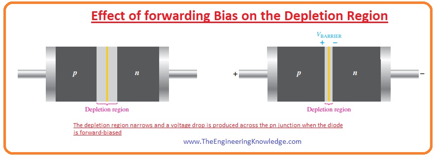
Effect of the Barrier Potential During Forward Bias:
Above we discuss that the depletion region consists of the positive and negative, and these are linked with each other through the electric field.
And this field makes an energy barrier for electrons and holes to cross the depletion region. This energy barrier is called a potential barrier.
When the diode is connected with the forward-biassed condition, then the electrons get the energy to cross the barrier to move the P side.
The energy provided by the battery is equal to the potential barrier.
Diode Reverse Biassing
In reverse biassed conditions, current does not flow, or a very small amount of current flows.
In a reverse biassing situation, the positive terminal of the battery is attached to the cathode, and a negative terminal is attached to the anode of the diode. It is shown in a given figure.
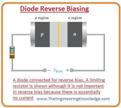
- The voltage source connected in this reverse biasing is denoted as Vbias.
- In the above figure, you can see that the area of the depletion region is wider than the depletion region of forward biasing.
- The process of reverse biasing is discussed with the detailed in the figure given below.
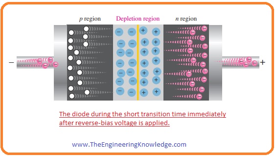
As opposite charges attract each other, the positive terminal of the battery attracts the electrons in the N regions, so due to the movement of electrons, further positive ions are created, and the area of the depletion region increases.
Similarly, electrons provided by the negative terminal in the P region of the diode combine with the hole and make negative ions, increasing the area of the depletion region.
With the increment in the area of the depletion region, the quantity of majority carriers in the P and N regions decreases.
Due to the large area of the depletion region, the ion strength of the electrical field is also increased, and there is no option for the flow of current, but there is a very small amount of current flow due to some minority carriers, but it can be neglected.
Reverse Current
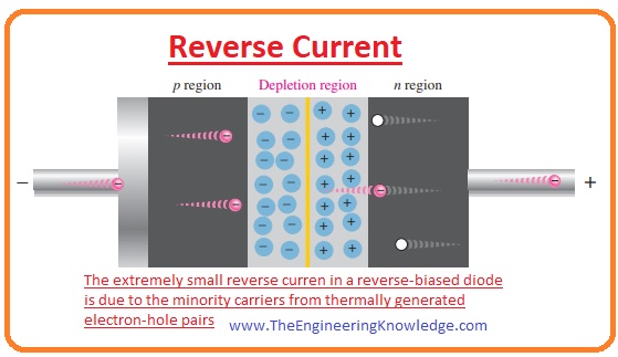
This current flows in reverse biasing conditions due to minority carriers existing in the P and N regions.
A small number of electrons present in the P region repelled by the negative terminal of the battery and moved towards the PN junction.
When the electrons reach the depletion region, they cross it and move to the P region. Due to this movement, a small amount of current flows. This current is called reverse current as it flows through the N to P side of the diode.
The figure given below explains the movement of reverse current in the opposite direction. As opposite charges attract each other, the positive terminal of the battery attracts the electrons in the N regions, so due to the movement of electrons, further positive ions are created and the area of the depletion region increases.
Similarly, electrons provided by the negative terminal in the P region of the diode combine with the hole and make negative ions, increasing the area of the depletion region.
With the increment in the area of the depletion region, the quantity of majority carriers in the P and N regions decreases.
Due to the large area of the depletion region, the ion strength of the electrical field is also increased, and there is no option for the flow of current, but there is a very small amount of current flow due to some minority carriers, but it can be neglected.
Reverse Current
This current flows in reverse biasing conditions due to minority carriers existing in the P and N regions.
A small number of electrons present in the P region repelled by the negative terminal of the battery and moved towards the PN junction.
When the electrons reach the depletion region, they cross it and move to the P region. Due to this movement, a small amount of current flows. This current is called reverse current as it flows through the N to P side of the diode.
The figure given below explains the movement of reverse current in the opposite direction.
Reverse Breakdown
Usually, the reverse current is very small and not taken into consideration, but if the input voltage is provided at the level known as breakdown voltage, then the reverse current flows very largely.
After getting energy from the voltage source, minority electrons in the P regions move towards the potential barrier; during their movement, they collide with other atoms, releasing the valence electrons from those atoms.
The released electrons also collide with other atoms, and further electrons are released.
So this process makes minority electrons into the majority, and they move to the N region after crossing the potential barrier.
The increment in the number of free electrons is called the avalanche effect, so the quantity of reverse current increases due to the avalanche effect.
If this reverse current is not in the limited condition, it can damage the diode.
Difference between Diode and LED
Now we discuss the difference between a diode and an LED in detail.
| Diode | LED |
| A diode is used to provide rectification and operate only in one direction. | LED stands for light-emitting diode. When a voltage source is connected with it emit light. |
| It is manufactured with silicon and germanium. | It is manufactured with the GaAs and GaP. |
| It transforms energy into heat. | It transforms energy into the light. |
| Its reverse breakdown voltage is large. | Its reverse voltage is less. |
| It starts operating at 0.7 incase of silicon and 0.3 in case of germanium | It operates at 1.2 to 2 volts. |
| It used to rectifier ac into dc. | it used to produce light |
| It used as rectifies, clamping circuits, etc | It used as a light source, as an indicator in the seven-segment display. |
Difference between Diode and Photodiode
- Now discuss the comparison between diode and photodiode.
| Diode | Photodiode |
| It operates only in forward biasing. | It operates in reversed biased mode. |
| It operates as a switch | It transforms light into electrical current. |
| Constructed with the silicon and germanium | It also constructed with germanium and the coating of silver nitride is used as anti-reflective. |
| It used for rectification, clamping circuits, etc. | It used in optical devices like cameras, etc. |
Difference between Diode and Zener Diode
- These are some differences between diode and Zener diode.
| Diode | Zener Diode |
| It operates only in forward biasing. | Zener diode operates in forward and reverse bias conditions. |
| If it operates in reverse biased condition, it will be damaged. | It will operate in reverse bias without any damage. |
| The doping level in a general diode is less as compared to the Zener diode. | I this diode is doping level is large to get a high value of breakdown. |
| It used for rectification, clamping circuits, etc. | It is used in voltage regulation circuits. |
Difference between Diode and Transistor
- These are some differences between the diode and the transistor.
| Diode | Transistor |
| A diode is 2 terminal device used to allow current to flow in a single direction. | A transistor is a 3-terminal device through which current flows from a high-resistance area to a lower-resistance area. |
| In the construction of a diode, only two semiconductor materials are used P and N. | In a diode, three layers of semiconductors are used one is between two semiconductor material either P or N and makes a combination of NPN or PNP transistor. |
| In a diode is only a single depletion region | A transistor has 2 depletion regions. |
| A diode has only a single junction among P and N material. | It has 2 junctions first is between emitter and base and second between base and collector. |
| A diode has 2 terminals positive called anode and negative called cathode. | Three terminals in transistors, known as emitter, base, and collector. |
| It can work as a switch. | It can be operated as a switch and amplifier. |
| It operates as a switch in clamping circuits and rectifier. | It operates as an amplifier and an oscillator. |
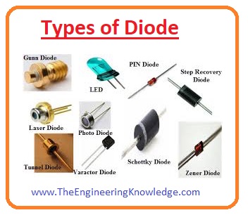
Types of Diode
- There are numerous types of diodes lets discuss them with the detailed.
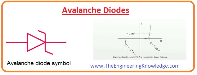
Avalanche diodes
- The operation of these diodes occurs when the reverse-biased voltage crosses the breakdown voltage.
- The operation of these diodes is almost similar to the Zener but with some differences in the breakdown effect that is an avalanche effect.
- It occurs when the reverse voltage provided cross the potential barrier, and current start to flow in large amounts, like an avalanche.
- The structure of these diodes that do not allow them to damage at the reverse biased condition.
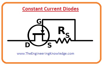
Constant Current Diodes
- This diode is also known as a junction field-effect transistor (JFET) its gate terminal is attached to the source.
- So it operates like the voltage-limiting Zener diode.
- This diode is also known as CLD (constant current diode) due to the linking of transistors.
Crystal Diode
- This diode is also known as point contact diode when the first time it constructed for use in the receiver of microwaves.
- The working of this diode relies on the pressure between point and the semiconductor substances used in its construction.
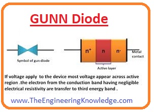
Gunn Diode
- This diode is also known as a transferred electron device (TED) it has negative resistance with the 2 terminals.
- It used in such electronic projects where the high frequency is required.
- It used for the generation of microwaves in electronic oscillators.
- Due to microwave generation, it is employed in RADAR, microwaves and automatic door openers.
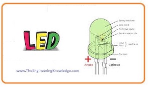
LED
- An LED stands for light-emitting diode it releases light when input supply is provided to its terminals.
- The process of light emission is accomplished when the electrons move from the N side to the P side and combine with the holes.
- When electrons combine with the hole they release their energy, and this energy is emitted in the form of light.
- The color of the emitted light depends on the semiconductor material used for the construction of LED.
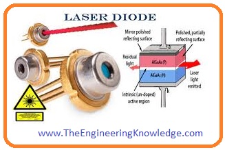
Laser Diode
- A laser diode (light amplified by stimulated emission) diode also called an injection laser diode.
- It also emits light similar to the diode but the emission process is different. It uses the spontaneous and stimulated emission processes for the emission of light.
- The working of a laser diode is mentioned previously you also read it in detail. Laser Diode
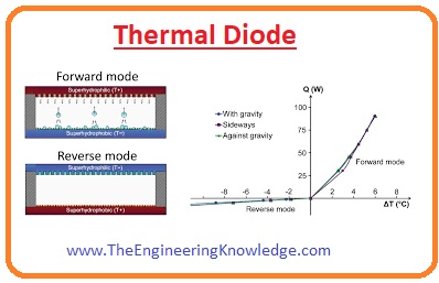
Thermal Diode
- This diode is similar to a normal diode and allows current to flow in only one direction like current flow in a normal diode.
- It is used in a heat engine, refrigeration and some other heat transfer-related applications.
Photodiode
The type of diode transforms light into the current. The photons of light collided with the photodiode and are converted into the current.
With the increment in the surface area, its response time decreases. The practical example of a photodiode is a solar cell that uses numerous photodiodes for the conversion of light into the current.
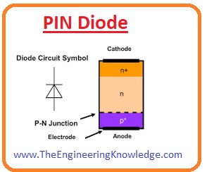
PIN Diode
The operation photodiode is alike to the photodiode that transforms the light into the current.
There are 3 main parts of a PIN diode: first is P, second is I (intrinsic), and third is N region.
The intrinsic region is sandwiched between the P and N that are heavily doped semiconductor materials.
A PIN diode is used in different switching circuits, photdetecting devices, and large power-consuming electronics instruments.
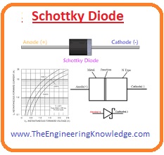
Schottky Diode
- This diode is manufactured with a metal and a semiconductor material. The forward-biased voltage drop of this diode is less as compared to the general PN junction diode.
- The value of forward voltage loss at a current of one milliampere is in the range of 0.15 volts to 0.45 volts, due to this feature it is used in clamping circuits.
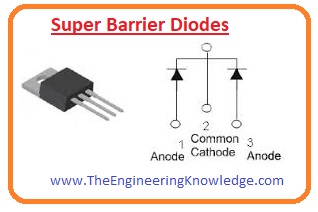
Super Barrier Diode
- This diode is used in rectifier circuits were due to less value of forwarding biased voltage loss and better surge-handling capacity.
- It also has less value of reverse leakage current than a general diode.
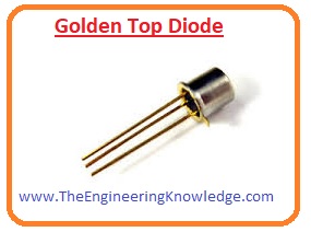
Gold Top Diode
- In this diode, gold is a dopant material in some diode platinum is also used as a dopant material.
- The use of gold increases the movement of electrons from the N region to P region.
- The operation of a gold diode is fast than that of the other diode but less than that of the Schottky diode.
- The value of leakage current is less than that of the Schottky diodes.
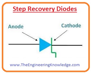
Step Recovery Diodes
- This diode is also called a voltage-dependent variable capacitor. Its doping level is very less close to the PN junction.
- Also, the quantity of carriers is little nearer to the junction.
- This diode operates very fast at less frequency values, so it is also used as a charge-controlled switching circuit.
- It operates in forward bias and does not operate in a reverse-biased circuit.
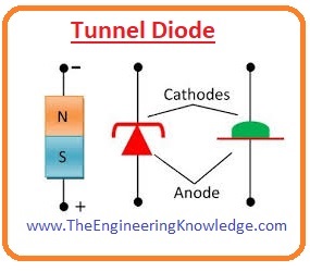
Tunnel Diode
- This diode has features with which the increase in voltage-current decreases.
- It used in computers due to fast switching and also used in high-frequency amplifier circuits.
- The other name if this diode is the Esaki diode due to its creator’s name.
Varactor Diode
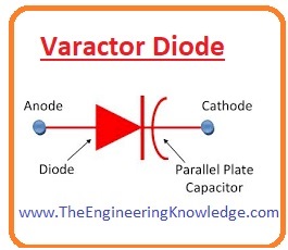
- The word varactor is derived from the variable capacitor. This diode only in reverse bias.
- It is similar to the variable capacitor during its reverse biasing.
- There are some other names of this diode like varicap tuning and variable capacitance diode.
Applications of Diode
- Friends, I hope till now you have become well aware of the diode; now let’s discuss practical applications of diodes with the detailed.
Radio Demodulation
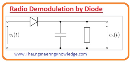
- The first time a diode was used in a circuit for the demodulation of AM radio signal.
- Amplitude modulated or AM wave comprises of the positive and negative peaks of radio waves as a carrier, the magnitude of this wave is equal to the audio.
- The diode only rectifies the amplitude-modulated radio signal.
- After that, the sound is separated from the carrier signal by using a filter and provided to the transducer to conversion into a sound signal.
Power Conversion
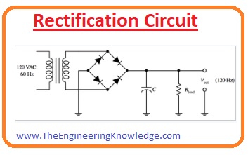
- The diode used as a rectifier in which it transforms the AC signal into DC this process is called rectification.
- The given circuit shows the rectification process of the diode.
Logic Gates
- Diodes are used to construct logic gats by combination with other instruments.
Temperature Measurement Devices
- The diode is also used as a temperature computing device, a forward voltage drop of diode rely on the temperature.
Related Posts
- Current Regulator Diode
- Zener Diode
- Step Recovery Diode
- PIN Diode
- Schottky Diode
- Photodiode
- Varactor Diode
- Diode
- Zener diode Applications
- Laser Diode
- LED
So friends, that is the detailed post on the diode I have each and every parameter related to the diode. I tried my level best to make this post simpler and easier and describe every aspect of a diode. If you have any queries about diode ask in the comments. See you in the next interesting tutorial. Have a good day. Thanks for reading.