 Hello, readers welcome to the new post. Today we will discuss the Applications of Multilayer PCB. PCB board is a circuit board that is very commonly used in industries and different project creation. These boards are very commonly seen in electronic and electrical devices that have one or more copper layers. PCB board comes in different layers according to projects and design configurations such as a single layer, double layer, multiple layers, etc. The creation of a multilayer PCB design is a very important factor in getting reliable operation and signal transmission through the proper operation. If the design is not accurate and the material for the substrate is not accurate then the required function can not be obtained which causes the noise in operation.
If the PCB board is designed accurately reduces electromagnetic emissions and crosstalk which enhances the operating quality. As the construction of multilayer PCB is high and not easy to find the faults existing in the board due to the multiple-layer complicated structure. However, it provides good shielding and signal routing and offers numerous layout features for this board. In this post, we will cover the different parameters of Multilayer PCBs and learn about their practical applications. So let’s get started with Applications of Multilayer PCB
Introduction to Multilayer PCB
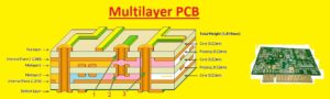
- Multilayer PCB is a type of PCB board that has more than two layers and a minimum of three conductive layers of conductive substance like copper material.
- When we analyze the structure of multilayer PCB then we will see that there is the same structure as the double-sided board but they have more layers about the core.
- The layer of these boards is connected through copper-plated holes and can be up to forty layers in multilayer boards.
- The components used for projects like transistors, diodes, resistors, and other components are connected to upper and lower layers of board and other central layers are used for routing
- These boards can configure more components mostly used in different devices and projects normally up to 12 layers of boards are used.
- Different smart modules use 4 to 8 layers boards such as a mobile phone having 12 layers.
- The construction of a multilayer board has an even number of layers than the odds
- For 4 layer structure to enhance EMI operation signal layers must be positioned as close to plans and apply a larger core among the power and ground plane.
- The firm compiling among the signal trace and ground plane mostly decreases the place impedance and also decreases common mode radiation through a cable attached to PCBs. This close trace-to-plane coupling reduces crosstalk among the traces.
- For board having layers of about 12 needs a thin dielectric and that results in tight coupling among layers.
- These boards are used for high-speed electronic operation to provide good EMI operation and signal quality.
- There is no limit to the number of layers on board you can construct according to design and requirements.
JLCPCB High-precision Multi-layer PCB
- JLCPCB is a high-level PCB-based service, provider. Founded in 2006, JLCPCB has been at the forefront of the PCB industry. With over 15 years of continuous innovation and improvement based on customers’ needs, they have been growing fast and becoming a leading global PCB manufacturer, that provides the rapid production of high-reliability and cost-effective PCBs and creates the best customer experience in the industry.
- Whether you’re building your first printed circuit board or developing an electronic hardware product, they are here to help you build hardware easier and faster by providing a rapid PCB prototyping and PCB assembly service. They are constantly looking for new ways to improve and shorten the PCB prototyping process – from a pioneering online quote/order system, and automated manufacturing to fast delivery.
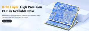
- JLCPCB currently provides a multilayer PCB service that has compatibility with twenty layers of the board. Multilayer boards are preferred for high-density board creation and in devices and projects that need accuracy and quality throughout the manufacturing process.
- So to fulfill all these features for your new project JLCPCB is the best option to get quality products at low prices.
JLCPCB Multi-layer PCB Advantages?
- The Multilayer PCBs of JLCPCB have many advantages.
- It is commonly used in complicated projects of electronic composite devices that have a high density of components and circuits.
- There is a need for more machines and details processes than other boards for the design and construction of multilayer PCBs. All these features enhance the chances to get high-quality boards. JLCPCB uses advanced solder mask LDI that provides reliable and stable solder mask bridges.
- There are no charges for “via-in-pad” with POFV for the 6, 8–and 20-layer circuit boards at JLCPCB. Free-of-cost POFV technique improves the efficiency of PCB design engineers. Since via has larger areas.
- As for these boards’ multilayer PCB stacks, layers exist on the upper side, so these boards can configure more components and circuits in a smaller space than other boards which reduces the size and weight of these boards.
JLCPCB Multi-layer PCB Uses Advanced Solder Mask LDI
- JLCPCB is the best in all services so they make sure to use high-quality equipment for all high-layer count boards.
- JLCPCB is a famous manufacturer that uses LDI technology for multilayer PCB that is very less common to apply by other manufacturers.
- JLCPCB high-precision LDI features remove solder bridge problems. For a similar pad gap when the pad opening is one mil single die, the pad bridge can be 6.66 mils provided by the JLCPCB advanced LDI machine.
- So problems are solved through PCB design, in this way JLCPCB can deal with assembly irrespective of the density of the IC gap.
- Ulta high-precision alignment solder mask LDI is used for four to twenty-layer PCB orders, whether they are small batch or high orders, and whether engineering charges are paid or not.
- Single and double-layer PCBs are monetarily created through a CCD automatic alignment exposure instrument that is not compatible with these solder mask opening designs and has compatibility with multilayer designs with four to twenty layers
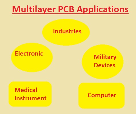
Multilayer PCB Applications
- The main applications of these boards are explained here
- These boards are used in mobile phones smart modules and some other electronic devices size they as the ability to handle more components on small structures.
- In a communication system, there are different conditions like high-temperature low-temperature pressure, and other factors to be faced by the component so these boards used in this industry
- This board provides durable operation and the ability to handle high pressure and temperature so used in industries and heavy machines
- Their robust and less weight functions help to use them in different medical devices and instruments like X-RAY machines etc
- These boards are used in military and defense instruments and machines used in the army.
- These boards are also used in the automotive and aviation industry.
Related Posts
- Aluminum PCB (Printed Circuit Board)
- Multilayer PCB (Printed Circuit Board)
- Rigid PCB (Printed Circuit Board)
- Flex PCB (Printed Circuit Board)
- High Frequency PCB (Printed Circuit Board)
- Single Sided PCB (Printed Circuit Board)
- Rigid-Flex PCB (Printed Circuit Board)
- Double sided PCB (Printed Circuit Board)
That is all about the Applications of Multilayer PCB all details have been explained if you have any questions ask them here. Thanks for reading have a good day Read our More Engineering Blogs


