 Hello, friends, I hope all of you are enjoying your life. In today’s tutorial, we will have a look at Double Sided PCB Board. PCB stands for printed circuit board, it is thinner chip constructed by the epoxy, fiberglass or some other laminated substance. On this circuitry board, there are numerous paths are manufactured that for current movement and numerous components for any circuitry can be assembled on these conductive paths. Components like resistances, transistors, capacitors or some other ICs can be assembled on this board.
This board has lots of practical applications in electronic devices and projects, like computers, laptops, mobiles, calculators, are consist of this circuit board, in computer example of PCB is its motherboard on which different components are assembled. There are numerous types of PCB according to construction and uses like, single sided, multilayer, rigid, rigid-flex, flexible PCB, etc. In today’s post, we will have a look double-sided its working construction, applications, advantage, and disadvantage. So let’s get started with what is double sided PCB board.
Double Sided PCB Board
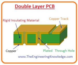
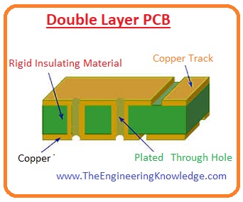
- The double-sided printed circuit board is also defined as a double-layer board as it provides on both side conductive paths for assembly of components.
- On this circuit board, both sides are covered or coated with current-carrying (conductive) material like copper.
- The main feature of this board over the single-layer board is that on this board there is a hole though which components of one side can be connected with other side.
- For the connection of components on this module there are 2 method used first one is surface mounted and second one is through hole. Both of these have their advantages and disadvantages and can be used according to the user’s requirements.
- In the through-hole connection technique, the small wire are passed through holes and joins different components.
- But in surface mounted technique there are no separate wires used to link components but in this method on the surface of board wire already soldered to provide conductive paths, this method provides uses less space for components assembly and decreases the weight of the board.
Construction of Double Layer PCB
- Construction of this circuit board is alike to the single-layer circuit board, its construction is described here with detailed.
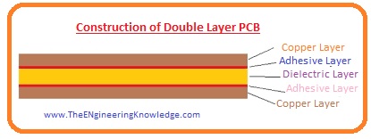
- In this circuit substrate is manufactured by the glass fiber or epoxy resins, the type of base material relies on rigidity and flexibility of board.
- In this double layer, PCB over base substance copper lamination are done to provide conductive paths for components.
- To provide protection from the environment both sides of the circuit board comprises of a solder mask over the copper covering.
- To an easy understanding of the circuit board for new users, there are different symbols of components that are already designed onboard over silkscreen that is above the solder mask.
Double-sided PCB Board Applications
- Due to simple design and easy to handle there are some practical applications of this board that is described here.
- with the use of this board in technical devices, these are also employed in medical devices like X-ray machines, CT scan, pacemakers are consists of this circuit board.
- In industries, this board also has numerous applications in different machines and instruments.
- Different converters like analog to digital or digital to analog uses printed circuit boards for their circuit assembly.
- Different control relays are also comprised of this Pcb.
- In different power converter circuit it uses.
- In HVAC (heating, ventilation, and air conditioning) this board also used.
- Different lighting devices like light-emitting diodes are consists of circuit boars.
- Differed power supplier circuits also consist of these PCB boards.
- Voltage regulators also consist of this board.
- UPS is a common useable device in our home and offices it also uses PCB for circuit assembly.
- Different traffic control circuits also comprise of this module.
- Vending machines also used this PCB board.
- Your personal computer motherboard also made with this printed circuit board.
- Vending machines also comprises of these boards.
- Line reactors circuitry also uses this board.
- Printers also comprise of this board.
- Your cell phone also consists of this board.
- Different amplifier circuits also consist of this board.
Advantage of Double Sided PCB Board
- This PCB board is very general for manufacturing and prototype circuitry. These boards provide an easier way to constructs different conductive paths on boards.
- Like single-sided circuit board, this board also consists of an insulating material and over it, on both sides, copper layers are deposited.
- Due to both the conductive side, you can assemble a large no of components and ICs.
- Another benefit of using double layer PCB is the augmented heat dissipation that an additional layer of copper offers, this can be attained in the engraving procedure, only eliminating enough copper to make the tracks, leaving the additional copper instead of eliminating it entirely.
- The choice to use double-layer PCB desires to be considered very sensibly, since the additional complication in construction and handling of the board, as well as the price, can make using a double layer PCB a sub-optimal option to use in different engineering projects.
- The main deliberation is production price since maximum producers will charge additional setup dues for handling the additional side, not only on engraving and solder mask but also on constituent designs added in the silkscreen processing.
- Other additional expenditures could originate from the design procedure itself, as numerous extra design deliberations should be taken into notice to confirm proper operation of the complete product, like inductive damages and stray capacitance upsetting the working of analog and high-speed digital circuitry.
Related Posts
- Aluminum PCB (Printed Circuit Board)
- Multilayer PCB (Printed Circuit Board)
- Rigid PCB (Printed Circuit Board)
- Flex PCB (Printed Circuit Board)
- High Frequency PCB (Printed Circuit Board)
- Single Sided PCB (Printed Circuit Board)
- Rigid-Flex PCB (Printed Circuit Board)
- Double sided PCB (Printed Circuit Board)
So friends that is the detailed post on the double-sided post I have written each and everything related to this module with the detailed. If you have any questions about it ask in comments. See you in the next tutorial.


