JLCPCB Best PCB supplier

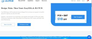 jlcpcb easyeda collaboration
PCB prototyping is considered is the main component to make any electronic based project and device and EDA is used to make the design of that project
 Top reasons to get pcba service from jlcpcb
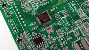
PCBA stands for Printed circuit board assembly is complete packaging that comprises of all types of components at the board for practical usage.
 PCB Prototype Service by JLCPCB
prototype of PCB boards is like a demo board that is used for checking the circuitry of the projects that we are going to make.
 How to Design PCB From JLCPCB
There are some steps that have to follow for the design of PCB First, create the structure of your board using the EsyEDA software that is a PCB design tool. To make a design at the software you must has an account if you have no account make a new one and move to their site.
 How to Get PCB From JLCPCB
For designing the board there is the use of EasyEDA software that is normally used by engineers, and students of technical backgrounds for designing their projects.
 Top Reason JLCPCB Best PCB Supplier
This PCB manufacturer is JLCPCB which is china based PCB supplier and was founded in 2006. It collaborates with EasyEDA so you can get two services on a single platform. More than three thousand employees are working in this company and offering all over the world services.
 How to Manufacture PCB Board
PCB board is the very basic component of each and every electronic device and electronic project that is created or constructed in any field of engineering.
 Best Online PCB Manufacturer JLCPCB
JLCPCB is the largest manufacturer of the printed circuit board and its head office is located in china it has the capacity to create a simple design of PCB to multilayer PCB design.
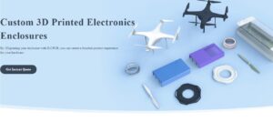
 3D Printed Parts From Best Supplier
To the creation of different types of projects, there is the usage of digital model files in the three-D printing technique. The benefit to using this technique is the printer creates or does the printing of the complete module in some hours by taking into consideration the complication of design
Top Reason to Choose JLCPCB for Project Manufacturing
JLCPCB is china based PCB manufacturer that offered different services related to PCB and PCBA. It was established in 2006 and offering services to its customers for the last twenty fourteen years. They are not serving to local customers but all over the world and follow the IPC 7351 standards
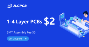
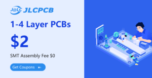
 Aluminum PCB Assembly in 2$
Aluminum PCB is constructed by aluminum and has a high heat dissipation factor so it is mostly used in lighting products like light-emitting diodes.
This module has 2 sides on the first side that is white in color is have numerous light-emitting diodes and the other side aluminum is used.
 PCB Design with EasyEDA & JLCPCB
JLCPCB and EasyEDA belong to one big group or say they are sister companies. Meanwhile, designers can place their PCB order directly via EasyEDA after getting the design done.. To make the PCB design we will use a simple circuit of the project and make its design on the PCB board.
 HOW TO PLACE FIRST ORDER ON JLCPCB
JLCPCB offers high-quality boards at affordable prices. They are compatible with the god services for different projects to their customers. High-quality products are always preferred by the users.
 How to get Low Cost SMT Service by JLCPCB
PCB board is a very basic part of electronic projects where different types of boards are created and used. For the creation of PCB boards, there are different techniques
 Why JLCPCB is the Best SMT Provider
SMT is a technique that is used for the creation of board by connecting the components on the board. This technique is very commonly used currently for board creation. In this technique components
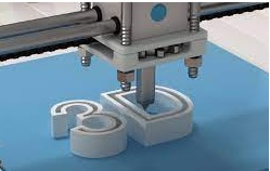 Industrial 3D Printing by JLCPCB
Three-D printing called additive manufacturing is a technique used to create 3D objects through the use of digital data. The additive process is used for the creation to 3-dimensional objects. Three-dimensional printing is the contrary process of the subtractive manufacturing process that cut pieces of metal through the use of milling machines.
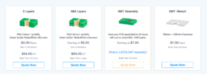
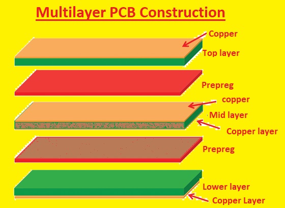 Applications of Multilayer PCB
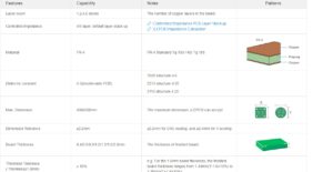
Multilayer PCB is a type of PCB board that has more than two layers and a minimum of three conductive layers of conductive substance like copper material.
When we analyze the structure of multilayer PCB then we will see that there is the same structure as the double-sided board but they have more layers about the core.
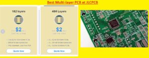 Best Multi-layer PCB at JLCPCB
The multilayer PCB has a minimum of three layers in the structure of conuctuve material like cooper. Between these copper layers, there are insulated materials used to avoid damage to conductive layers due to high temperatures during circuit working.
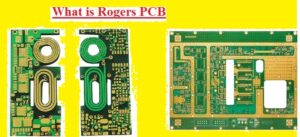
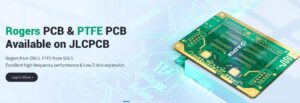 Rogers PCB & PTFE PCB: High-Frequency PCB is available on JLCPCB
In this post we will discuss Rogers PCB & PTFE PCB: High-Frequency PCB is available on JLCPCB. The high-frequency board is the best option for projects like signal transmission among two different devices. This PCB board uses certain types of materials for attaining
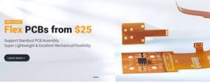 Flexible PCBs: The Future of Electronics Manufacturing
Flexible PCBs sometimes referred to as flex circuits or flexible circuits, are a creative solution that offers electronic devices a great level of design freedom and dependability.
 Roger Material: The Ultimate Solution for High-Speed and High-Frequency PCBs
A printed circuit board known as a Rogers PCB employs Rogers material as its primary substrate. A high-frequency laminate known as the Rogers material is made of a combination of glass, ceramic, and polymer components.
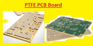
PTFE PCBs: The Ultimate Solution for High-Frequency Applications
PTFE, or polytetrafluoroethylene, is a type of thermoplastic polymer this is used in different industries due to its superb thermal, electrical, and chemical houses. Whilst utilized in PCBs, PTFE can offer superior performance compared to different substances due to its high dielectric regular, low loss tangent, and fantastic thermal stability.
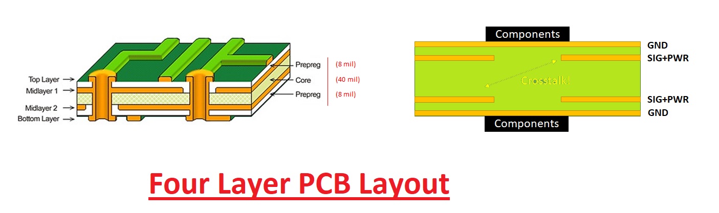 Four Layer PCB Layout: Design Process and Cost of Manufacturing
A 4-layer PCB is a printed circuit board that comes with four layers of conductive material separated by insulating layers. It belongs to multi-layer PCB that offers increased flexibility and good performance compared to single-sided or double-sided PCBs
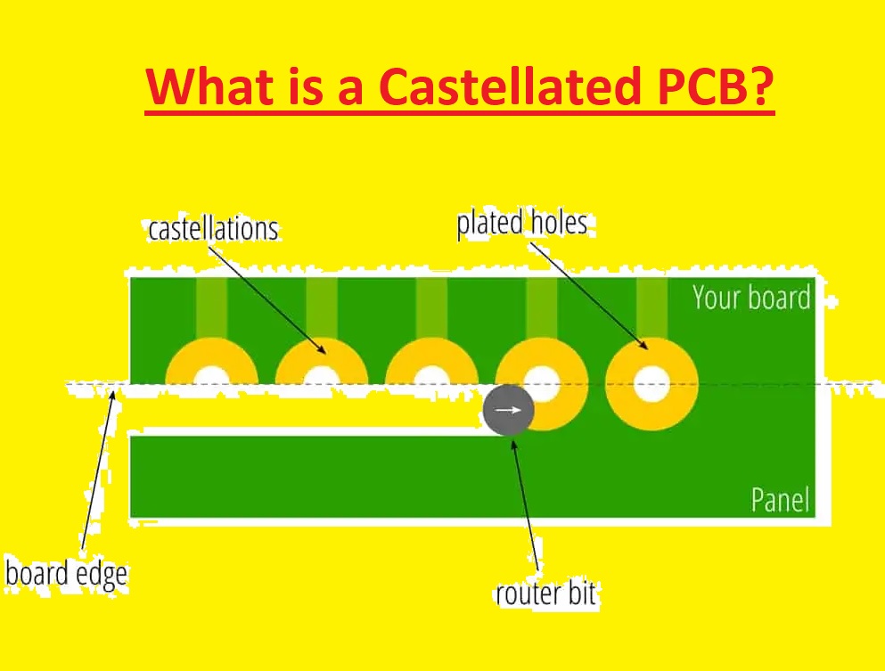 How to Design a Castellated PCBs Board in 2023
A castellated PCB is PCB type that features plated edges on one or more sides. These plated edges normally come with a pattern of half-holes, resembling the battlements of a castle, so they are known as “castellated.”
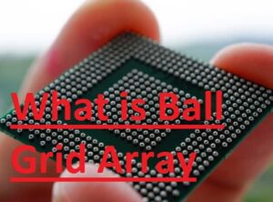 What is Ball Grid Array (BGA) on a PCB Board
BGA is a surface-mount packaging type where solder balls are configured in a grid-like pattern on the bottom of a component. These solder balls create electrical connections between components and the PCB board.
 Importance of Copper Pour in Empty Areas on PCBs
When designing boards, engineers strive to enhance their functionality, reliability, and performance. The copper pour is a method that helps achieve these goals with the use of the empty areas on the board to enhance its overall performance
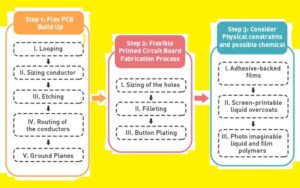
What are the Steps Flexible PCB Manufacturing Process
Flexible boards provide many advantages that make them best for various industries. Firstly, their flexibility is used for seamless integration into compact and irregularly shaped devices, optimizing space use. 2nd, their less-weight nature decreases the total weight of the electronic assembly.
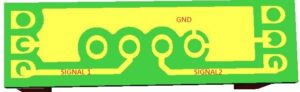
 Overview of Flex PCB Panels: Definition, advantages, and Applications.
A flex PCB panel, also called a flexible printed circuit board, is a PCB board that is constructed with the use of flexible substrate materials, like polyimide or polyester films.