SONY DSC
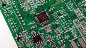
Hell readers I hope you all are enjoying your life. In this post, we will learn How to Manufacturer PCB Board. PCB board is the very basic component of every electronic device and electronic project that is created or constructed in any field of engineering. So the proper working and construction of any PCB board is needed appropriately so our project works accurately and properly since its main requirement is to work effectively.
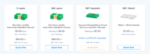
In this post, we will learn how we can make our PCB for project simulation. If you are new and have little knowledge of PCB construction here I want to mention that you can get the services of different PCB manufacturers but I want to suggest the best PCB supplier and manufacturer that make PCBs at the proper level and best prices with good quality that are easily getting by any users and will also learn how PCB manufactured in JLCPCB. This PCB supplier is JLCPCB. It is China-based PCB supplier that has been offering PCB services for the last fifteen years all over the world. They never compromise the quality and best services that you need. Their main services are related to PCB, PCB prototyping with different types of boards like single-sided, double-sided, multiple-sided PCBs, etc. JLCPCB is continuously driven to become more efficient and reduce costs. they promise to offer customers the most economic PCBs forever. They are constantly looking for new ways to improve and shorten the PCB prototyping process from pioneering online quoting systems, and automatic production to fast delivery. Almost more than three thousand employees consisting of engineers and other staff is working in their industries. Some interesting offers offered by the JLCPCB are shown in the below figure. So let’s get started on How to manufacture PCB boards.
How to Manufacturer PCB Board
- There are some steps needed to make PCB that are explained here in detail.
PCB Film Design
- When any customer sends the Gerber file to the JLCPCB their engineer reviews that file and comes to know that either it is ready to make PCB or has to amend it.
- file gets accepted this design is created through the use of photoplotters and created in the photomasks in a certain value of temperature.
- info is given in the Gerber by the photoplotter and transforms into image form.
- It is a film that is sent for manufacturing procedure.
Material Cutting for PCB
- In this step, the material that will be used for PCB construction is FR4 used in different ranges of thickness like 0.4, 0.6, 1.2, etc, and has copper sheet covered at both sides working as lamination.
Drilling Process
- In this process, holes are created through the use of drilling through which components lead passed and connection will be made.
For the accuracy of holes at the boards, there is some additional holes made at the corners of the boards.
The drilling machine is software-operated different software is used to design the holes according to PCB configuration.
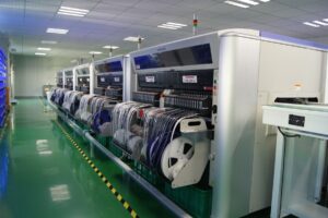
In the factories of JLCPCB, there are almost seventy drill machines available.
Copper Placement
When drilling is completed then an electroless deposition procedure is employed that helps to place the copper at the board and make different layers of copper that will help to the movement of current in the project that will be created on it.
There is plated through holes are used to make connections between conductive elements placed in the copper layers.
External Layer Imaging
This procedure also called dry film etching where the board is covered with a thin sheet of material called photosensitive etch resist.
After this board is placed in areas where UV light falls on it.
The UV light will make strict the photoresist placed at the board.
Additional resist element is removed from the board and the board is placed in a high temperature where the operation time of other resistant materials increases.
Plating Process
For increment in the copper thickness that lies at the board and about the holes, is plating process is done on the board. There is a layer of tin is placed at the board through plating.
When the plating is finished resist element is completely removed and just copper layers, pads, and plated layer remain at the board.
Etching Process
In the etching process, the additional copper that exists at the board is removed and does not affect the plated area.
After that plating is removed with the use of the solution of chemical substances and just remained the copper layers pads and holes at the board.
Automated Optical Inspection
It is a visual inspection technique that is used to find the different faults that occur at the board and areas where resist elements get removed with the force and make a scratch.
These types of errors can not be removed through continuity tests. In the visual inspection technique, there is the usage of the laser.
Solder Mask Usage
To protect the boards from the external environment and harsh conditions there is the employment of solder MASK on the board.
Its normal colors are blue, red, white, and yellow.
Silkscreen
Silkscreen is very useful for users to get the proper knowledge about the layout of elements that are employed at the board.
In this process, there is numerical numbers, alphabetical letters, date of creation, and features of components are mentioned at the board.
Silkscreen can be employed at the lower part of the board.
Surface Finishing
In this process, PCB is plated through the use of electroless gold over nickel. It has two benefits first one is to protect the copper to get corrosion and the second one is offering a solderable area to position the circuit components.
Profiling Process
In this process is certain shape is given to the board through the use of a machine operated with the computer.
There is a smooth corner is given through this process. There is the usage of V cutting for isolation of board.
There is the use of a cutting device for the creation of a V form line at the board. It helps to board snapped out.
Electric Testing of board
An electrical test is done on the board to find any fault or open circuit in the board and there is a short circuit.
Final Inspection
When the board is completed at the JLCPCB is final review is done to check whether all requirements of customers exist in the board and if there is no fault in the board. The board is sent to the customer.
Read also:
- How to Reduce the PCB Board Size for Projects
- What is PCB Leds Circuit Board: What Do You Need to Know
- Learn How PCB Circuit Board Soldering Guide for Beginners
- How to Design a Castellated PCBs Board
- What is Ball Grid Array (BGA) on a PCB Board
That is all about the How to Manufacturer PCB Board I tried to cover the all steps involved in the PCB manufacturer if you have any queries ask in the comments. Thanks for reading have a nice day.


