 Hi, friends welcome to a new post in this post we will discuss How to Design PCB from JLCPCB. The design is a very important part of any project creation as all elements of that project have to be configured at the board. If the board is not accurately designed and created then the project will not be created accurately and will not function well. So the designing of the board is done in a certain condition that is favorable for design and makes your projects well.
For that purpose, we must be well-equipped and have sound knowledge of PCB design if not design does not get well. If you do not has any proper knowledge of designing you must get the services from a PCB designing company that can provide wellness services. For that purpose here i am going to suggest such a PCB supplier and PCB designer that offers PCB design services is JLCPCB.
It is chinas Chinas-based PCB supplier and offering services for the last fifteen years and has almost three thousand employees that work in different departments. They also serve all over the world at different prices that can be afforded by the users. Since 2006, JLCPCB on regular driven to become more efficient and reduce costs. They promise to offer customers the most economic PCBs forever. JLCPCB makes the cheapest but top-quality PCBs possibly because of scale effect, extremely high production efficiency, and less manpower cost. Their advanced PCB technology permits them to offer high-precision boards suitable for industrial, military, aerospace, and medical applications. In his post, we will use for design the PCB EasyEDA that has collaborated with the JLCPCB and offered the design services. In this post, we will cover all the details through which we can get the details about the PCB design. So let’s get started.
How to Design PCB from JLCPCB
- Some steps have to be followed for the design of PCB
- First, create the structure of your board using the EsyEDA software which is a PCB design tool.
- To make a design for the software you must have an account if you have no account make a new one and move to their site.
- After making an account press at the Editor option and make a new project make the structure of your board and get the elements from the JLCPCB library to make structure at software.
![]()

![]()
- Use the wire option and get the accurate portion through the library and position in the screen of the software Now that the board structure is finished save it.
- In the next step choose the convert to PCB option from the tool list. A new screen will be shown positioned different elements in the screen and positioned.
- Try to place the components of projects as close so looks great.
- Save this work and initiate the routing process for this can be used manual routing tool and also use an autoroute option.
- Now send the Gerber file of your board to JLCPCB in this file all details of your boards have every is mentioned.
- Gerber file also has data related to layers of boards, width spacing dimensions, and traces.
- After doing the above steps open the JLCPCB site and make a free account if you are a new user.
- After login to your account move to quote now and upload the Gerber file.
- When you upload the Gerber file can see all the details of your boards. can see if your details are good or not.
- Now send the BOM and CPL files.
- After that select, the elements that you have to use in your boards get from the JLCPCB.
- After that make a final review of your board design and make sure that you have submitted all details and missing nothing and have some errors remove it.
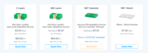
- In the final step complete your order for this press save to cart and select the shipping and payment method.
- Your order will be delivered in two to three working days if your needed instant projects will be delivered to you in twenty-four hours.
So that is all about the How to Design PCB from JLCPCB. I have mentioned every step to make a design from the JLCPCB if you have any queries ask in the comments. Thanks for reading have a nice day. Friends here I want to mention an interesting offer for you that I offering by the JLCPCB that is you can get a one to four-layer PCB board in 2 dollars for this click here.