Hello readers, welcome to the new post. In this post, we will have a look at the importance of copper pour in empty areas on PCBs. Copper pours are commonly used designs of printed circuit boards. It has empty filling areas on boards with copper planes that offer different advantages for electronic projects. In this post, we will cover different parameters of copper pour and its effect on board performance. Let’s get started with Introduction to Copper Pour.
Introduction to Copper Pour
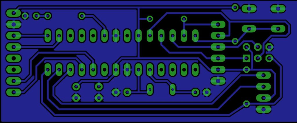
Copper pour defines the process of filling empty spaces on the PCB board with the use of copper. It defines the area of the board filled with the use of copper.
The copper pour is used to make the ground plane. It is an important factor since it helps board creators to optimize different features of design.
With quality copper pours, engineers can get high grounding, effective power distribution, and good electromagnetic shielding.
The main benefit of copper pour is best for optimal function of electronic devices.
Ground Plane Application
The ground plane is a special copper pour on board that works as a reference for ground connection. It is an important component in board designing since it has many advantages, like signal integrity, noise reduction, and electromagnetic compatibility.
The ground plane works as a low-impedance return path for signals and offers a stable reference for components on board.Here the importance of ground plane for the board is explained.
Signal Integrity:
- Signals on board can cause noise and interference that can affect the quality and performance issues. Ground planes mitigate these issues by providing uniform references for all components and traces on board. This board reduces voltage differential and signal reflections, making sure the signal is moving properly without distortion.
Noise Reduction:
- Electronic devices have chances to source noise, like EMI and radio frequency interference. The ground plane works as protection and reduces the effect of noise by offering a conductive barrier between sensitive circuits and external disturbances.
- It also absorbs undesired noise saves from coupling with signal traces and reduces the effect on circuit operation.
Wholesale PCBs SMT Stencil & PCBA Service Provider Special offer: $2 for 1-8 layer PCBs
Advantages of Ground Plane
The ground plane is made with the use of copper pours and is important for PCB design. It offers stable reference, enhances signal quality, decreases noise interference, and provides good EMC.
PCB engineers consider and apply ground planes to ensure optimal operation and reliable device creation.
The existence of a ground plane reduces signal reflection, provides impedance matching, and maintains signal quality in the board.
By offering protection from external noise sources, the ground plane reduces the chances of signals-to-noise interference and offers clean and reliable signal transmission.
Power Distribution Application
Efficient Power Delivery:
- Copper pours can be assigned to making power planes or board regions. These copper regions are connected with a power net and offer a less resistant pathway for power signals for different components reaching. By allocating enough copper areas for power distribution, engineers can ensure power delivery, reduce voltage losses, and make sure components get the required voltage levels.
Minimizing Voltage Drops:
- Voltage losses are caused when there is high loss across traces or power paths due to high resistance. Copper pours with low resistance provide good current flow and reduce voltage losses. By offering large and thick copper paths for high-power components, copper pours reduce impedance and resistive losses for power distribution and make sure components get the required voltage levels.
Prevention of Signal Integrity Problems:
- Accurate power distribution is important for signal quality; improper power supply causes voltage fluctuations resulting in signal degradation and signal quality issues. Copper pours help to solve these issues and power consistent power distribution on board.
How Does Copper Pour Affect Crosstalk and EMI?
Crosstalk Reduction:
- Pour reduces crosstalk through protection between sensitive signal traces. It covers traces with copper pours and an electromagnetic field produced through traces can be attenuated. It minimizes coupling signal traces and reduces crosstalk.
Ground Plane:
- These planes with copper pours offer differences for low impedance for returning paths in signals. It helps decrease the loop area of high-speed signals and reduces the returning path of signals. Ground plane also offers reference voltage and reduces ground bounce.
Impedance Control:
- It controls the impedance of transmission lines. Through setting width and copper pours, the configuration tune of impedance matches the requirement parameters. It minimizes signal reflection and enhances signal quality.
EMI Shielding:
- It provides protection for EMI. Covering components or traces in copper pour can reduce the cooling of the external electromagnetic field.
Copper Pours vs. Ground Pours
- Ground Plane:
- It is the inner layer of the board stacked up that is filled with copper and used as a signal power ground or reference.
- Ground Pour:
- The copper pour is used for grounding and does not cover the entire layer.
Importance of Copper Pour in Empty Areas on PCBs
JLCPCB makes high-quality boards with 5 intelligent manufacturing bases, cutting-edge machines, and raw materials. All PCB manufacturing processes are accurately controlled by JLCPCB.
Outer layer copper pour: 2- and multi-layer boards
When dry film is applied on boards, they put in a plating solution for electroplating with the use of fixed current.
Unused areas left blank
In effect of current, exposed copper that is not covered with dry film enhances thickness from copper in solution
Unused areas filled with copper pour
exposed copper at the time of this process comes with an effect on current distribution. Larger copper pours are used in PCB designs since they provide uniform current distribution.
Imaged PCBs ready for electroplating
In effect of current exposed copper that is not covered with dry film increases the thickness of copper in the solution
PCBs undergoing electroplating in an electrolyte bath.
Large areas of copper exposed for plating
if the exposed copper part of the board is small or not spaced out properly, it will bear different currents and come with varying plating thicknesses, through larger currents making a thicker plating. A supposedly 1 oz board comes with 2 oz of copper thickness as a result of this.
Not enough copper exposed during plating
The chemical process of electroplating
Electroplating makes 2 traces with less separation and no surrounding copper too thick to the point that dry film between is difficult to remove before etching. In result, extra copper exists between traces and causes short circuits.
Dry film remains between two closely spaced traces
Solution
For reduce quality standalone traces in design and distribute copper pour evenly on board. Design spacing between traces enough as part of standalone traces not configured with the copper pour. The designs that are faulty and good iterations are shown here
Copper pour has only partial coverage:
Before Improvement
After Improvement
No copper pour at all:
Before Improvement
After Improvement
Inner Layer copper pour: Multi-layer Boards
Cut the prepared in accurate size, but between two core layers or one core layer and one copper sheet layer, and then use high heat and pressure to assembly for melting and curing prepreg’s resin, which connects layers with each other
Prepreg
Inner layer core
Laminate
- Resin on Prepreg will extended to cover the copper-free zone if the copper layer comes with blank regions. it result in layer portion, voids in resin, folds in copper, and boards that are thin
A fold in a copper layer
Voids in a resin layer, visible from the white marks
Design example:
Before Improvement
After Improvement
2) The Goldfinger part is narrow than required if the inner layer part of Goldfinger is empty. It can result in poor connection between PCB and matching connection slot
1.6 mm nominal, 1.41 mm measured
Before: no copper pour in inner layer area of the goldfingers
After Improvement
Note: The importance of JLCPCB adding copper pour
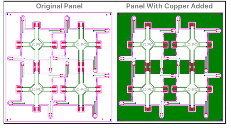
To avoid faults on larger empty areas like low board thickness and uneven plating. JLCPCB can use copper pour to panels on inner and external layers of multiple boards. Just handling strips, bridge components, and other points of PCB get copper pour. The boad not come with more copper practically. About fiducials, mechanical holes, mouse bites, and V-cuts, clearance will be added.
JLCPCB continuously works for consumers larger part of PCB manufacturing with use of the latest techniques. Not only JLCPCB provides one-stop PCBA from ordering quality boards to supplying 1 Million+ genuine electronic components and assembling boards with state-of-the-art SMT machines. Sign up at JLCPCB’s official website to get up to $60 new user coupons, start your PCB journey from here!


