Hi, friends welcome to the new post. This post will look at the Four Layer PCB Layout: Design Process and Cost of Manufacturing. The 4-layer PCB board is defined as a board that has 4 copper layers that are used for routing signals and distributing power. Stacking a 4-layer PCB accurately is needed to ensure good signal quality, reduce noise and crosstalk, and handle power distribution. So let’s get started 4 Layer PCB
What is a 4 layer PCB
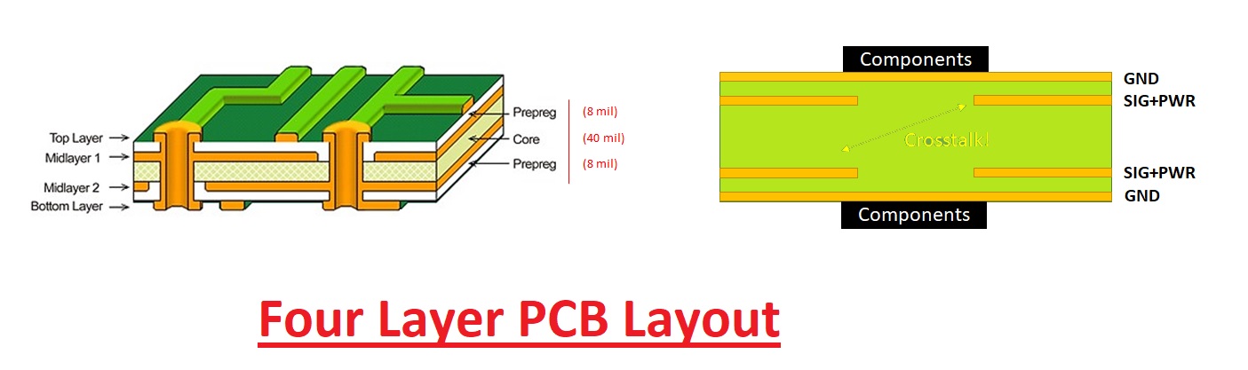
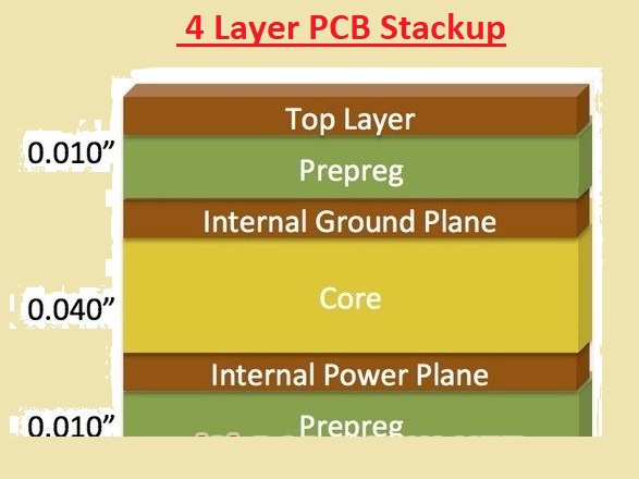
- The 4 layer PCB comes with four layers for routing electrical signals, that are Top Layer, Inner Layer 1, Inner Layer 2, and Bottom Layer.
- Upper and lower layers are called external layers, where components are connected and routed. Inner layer 1 and inner layer 2 are part of the core and are used for power planes and signal routing.
- So 4 layer boards come with 3 signal layers and a GND layer or 4-layer PCB = 2 signal layers + a VCC layer with a ground layer
4 Layer Stackup Configurations
Signal-Ground-Power-Signal
- It is a common stack-up used for mixed-signal or digital boards
- Layers use the upper layer 2 ground plane layer, 3 power planes, and lower signals.
- The ground plane offers protection between the top and lower signal layer, and the power plane provides power efficiently.
Signal-Power-Ground-Signal
- Another option is to swap power and ground planes
- Layer uses upper signals layer 2, power plane layer 3 is a ground plane, and lower layer.
- it is best to offer good power dissipation and maintain a grounding plane in the middle for protection
Ground-Power-Ground-Signal
- The board with high-speed or RF signals stacks up, having ground planes between the power plane used
- The layer used top ground plane layer 2, the power plane layer 3 ground plane and the lower layer.
- This configuration double ground plane avoids noise coupling and enhances signal integrity at high frequencies.
How to do 4 Layer PCB Routing
Four-layer PCB layouts come with differnt advantages than single-layer and double-layer boards
- Routing signals on internal layers to the ground plane is possible and offers shielding and isolation
- Route traces are orthogonally configured between layers to avoid overlapping traces and crosstalk.
- Flood not used part of a signal layer, having ground for offering protection and EMI reduction.
- Use vias for transition signals between layers and reduce the number of vias used.
- Try to avoid routing signals through cutouts in power planes. It can cause noise coupling.
- Use thick traces for high-current power nets, for connectors.
- Use stitching vias about the edges of the board for the connection of ground and power planes. It provides a bypass.
- The route traces at 90 degrees to slots or openings in planes. Try to avoid signals in parallel configuration with slots.
- Apply blind and buried vias for optimizing routing in internal layers.
- Check RF designs for transmission line effects. Control impedance through trace width
Example 4 Layer PCB stackups
Digital Electronics Board
This board comes with digital and analog circuits and is needed for handling moderate-speed signals and power demands. The signal ground power signal stack up is used for
Layer uses upper digital and analog signal layer, 2 ground plane layers, 33.3V and 5V Power Bottom Mixed Signal Routing
The Ground plane operates upper and lower layers, and the power plane distributes many voltages
RF Transceiver Board
For maintaining signal quality for high RF frequencies, this wireless board uses a ground power-ground-signal stack up:
Top, ground plane, layer 23.3V Power Distribution Layer 3 Ground Plane lower is RF Circuits and Traces
Double ground plane protects RF components and trees from EMI and crosstalk.
High Speed Data Acquisition Board
Using different gigabit data channels signals ground signal power features used for
Use Top Analog Signals Layer 2 Ground Plane Layer 3 Digital Signals, lower 5V and 3.3V Power
It offers isolation between analog and digital signals and reduces interference.
$4.5/㎡ Off on Quality 4-Layer PCBs
JLCPCB is PCB famous supplier that offers manufacturing services to its clients. They are expert in high-quality and low-cost boards and also four-layer PCBs.
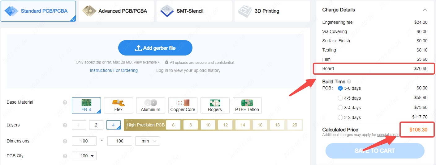
Now they have announced 4-layer PCB small-batch orders. You can get the benefit of a special discount of $4.5 per square meter, which lowers the board fee from $75.1/m2 to $70.6/m2. They come with a full film process for PCB production and use A-grade substrates, four-wire low resistance via checks, advanced solder mask LDI technology, and others. Put your order at the official JLCPCB website! Every new user will receive sign-up bonuses worth up to $54.
Calculate Your Savings for 4-Layer PCBs
Let’s use an order of 1 square meter as an illustration.
Through placing an order for 100mm*100mm 100pcs 4-layer PCBs with basic details on the JLCPCB online quotation page, you’ll find board prices of $70.60 and that the 4-layer PCBs will cost a total of $106.30. Compared to the market, you might save more than $100.
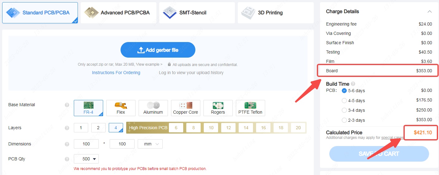
if you order five square meters.
The cost for an order for a 100mm*100mm 500pcs 4-layer PCB with basic settings is about $421.10, with the board costing just $353. On this order, you may save more than $300
The efforts made by JLCPCB on the production side have always been aimed at helping engineers worldwide overcome cost barriers in their pursuit of innovation.
Lower Prices, Same Quality
JLCPCB offers cost-effective solutions for PCB production without affecting operational durability and board reliability. Their main feature is based on JLCPCB 5 intelligence, making bases that continuously strive for increment.
With the use of accurate features, they optimize ineffective processes, increase the layout of PCB manufacturing lines, and use an automated intelligent management system. These features offer the best small-batch production of 4-layer PCBs.
JLCPCBhas been offering PCB manufacturing expertise to engineers and makers for many years, effectively transforming manufacturing advantages into a competitive edge.
Key Promises of JLCPCB Manufacturing’s Quality Focus
- All boards are made with use of a full film process without resorting to negative film.
- They use 4-wire boards like 4-layer PCBs, and employ LDI for circuit solder mas, providing equal-sized solder mask openings and good solder mask bridges.
JLCPCB Offers
- Flexible PCBs: offering a special cot for quality flex PCBs starting at $15.
- $2 special offer for 1-8 layer PCBs (5 pcs).
- Free assembly for 1-6 layer PCBs and for monthly redeemed SMT coupons.
- For high-frequency PCBs, the starting cost is $99.5 for Rogers boards (5 pcs) and $50.35 for Teflon boards (5 pcs).
Now $54 registration discounts are available for new users of JLCPCB. To avail this feature JLCPCB, sign up here.