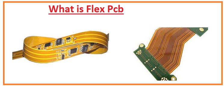
Hello readers, welcome to the new post. In this post, we will learn what the steps are in the flexible PCB manufacturing process. Flexible printed circuit boards are polyimide- or polyester-based PCB boards that can easily bend and fold. Flexible boards are single-sided, double-sided, black, white, and transparent. Light and thin are used where flexible structure is needed. So let’s get started with the flexible PCB manufacturing process.
Introduction to Flex PCB
PCB boards are now becoming the backbone of the electronic industry. It is mostly used in electronic products like computers, automobile electronics, industries, and different projects.
The main work is to support circuit components and interconnect circuit components.
FPC boards are a type of PCB board that normally have types based on structure and are single-layer, double-sided, and multiple-layer flexible boards.
Standard vs. Flexible PCB
The basic difference between a standard board and a flexible board is their material. Two main materials are used for flexible boards.
ABS is off-the-shelf plastic for normal manufacturing processes, making it easy.
Thermoplastic is a polymer that varies in structure with the application of heat or pressure. It makes materials such as PET and PBT malleable, strong, and relatively stiff.
It is used for the creation of less-weight components for aircraft.
The other difference is the manufacturing process. Flexible board manufacturing needs different processes than standard boards.
A special process is important for creating flex boards. Since it comes with molding, laminating, surface treatment, cutting, and bonding for final device creation.
Benefits of Flexible PCBs
- It can easily bend at 360 degrees.
- It is best for vibration resistance and can easily handle harsh conditions.
- It supports a compact and less-weight design, and it helps to reduce the project weight.
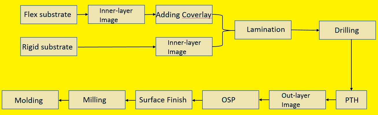
Steps in the Flexible Printed Circuit Manufacturing Process
Flex PCB Manufacturing Process & Advantages – JLCPCB
JLCPCB has started the flexible PCBs, which come with easy PCB assembly, and is now offering $25 for five pieces. JLCPCB has also provided $54 signup vouchers for new users at https://jlcpcb.com/.
JLCPCB Flex PCB Manufacturing Process
Flex Circuit Design:
First of all, make a design of a flexible board with the use of computer-aided CAD CAD software. The design comes with a layout of the circuit, component connection, and other features required for the bending of the PCB.
Material selection:
Proero substrate materials are selected for the board. PET layers and polyimides are commonly used by JLCPCB. They have a high resistance temperature and a flexible nature. Conductive paths are made on these materials. Since they are highly conductive and flexible, copper is used for layer creation.
Adhesive materials such as epoxy, acrylic, or silicone are used to connect layers of flexible boards.
Coverlay material: This material is used for the protection of conductive material on flex boards from environmental conditions like moisture, dust, and physical damage. Polyimide and polyester are commonly used coverlay materials.
Solder mask material:
This material is used for the protection of the conductive traces on board at the time of soldering. Solder mask materials are created with epoxy or photo-imageable materials.
Material preparation:
The surface of the substrate material is then cleaned and etched to provide a smooth, clean surface for the printing of the circuit.
Circuit printing:
The photolithography process is an important phase of flexible board manufacturing. This process comes with transferring circuit design from layout to substrate materials with the use of photoresist and etching.
First of all, get materials, then photoresist application, photoresist materials used on substrate surface.
The photoresist is a light-sensitive material that hardens when exposed to UV light. There are two photoresist materials for flex board manufacturing: positive and negative.
After that there is photomask alignment; the photomask is put on a substrate, and UV light is shone through a mask, exposing photoresist materials in the required pattern.
The photomask comes with a circuit design to print on substrate materials.
To UV light, the substrate is made to remove photoresist materials that are not exposed to UV light.
This process removes soft, unexposed photoresist material and leaves hardened photoresist that is related to circuit design.
The next phase is an etching that removes copper from there and is not protected with a hardened photoresist. It is done with an etchant solution that dissolves copper, leaving the required copper pattern on the substrate.
UV Exposure
Etching
Here, extra photoresist material is removed from the substrate with the use of a solvent that dissolves photoresist after the circuit has more substrate material, just printed circuit design on the substrate.
Component placement:
When the board pattern is printed, components on the board are connected. Components can be connected with the use of surface mount technology (SMT) or through-hole technology.
Soldering:
Components are soldered on board with the use of reflow soldering or wave soldering techniques.
Testing:
Different tests are performed to check the faults of the board and make sure that all components are connected accurately.
Flex PCB Testing
In the production of flex PCBs, the following testing techniques are frequently used:
Electrical testing:
This test checks the electrical connectivity of the flex board. The flex board is connected to a test fixture that applies voltage to the board and finds current. If any break exists or a short in the circuit is detected, the electrical features of the flex board are measured, like resistance, capacitance, and impedance.
Visual inspection:
It comes with an inspection of the flex board visually to find any faults like cracks, scratches, delamination, or misalignments. The inspection is made with a microscope or magnifying glass to make sure Flex PCB fulfills the required mechanical features.
Functional testing:
In this test, it is to make sure that it performs the required functions. The flex board is connected with a test fixture that simulates required uses, and working performance is measured for required specifications.
X-ray inspection:
In this test, with the use of x-rays on the inner layers of the Flex board, any error can be found, like a void or delamination. X-ray inspection is best for finding defects in the solder joints and hidden points of Flex PCB.
Advantages of Flex PCBs
Flexibility
Flexible boards can easily bend and flex without affecting the electrical connection of boards. It makes these boards best for uses that need bending or twisting, like wearable devices or automotive sensors.
Space Saving
Flex boards can be made for fitting in tight spaces as compared to right boards. It helps to use it for small and compact designs.
Durability
These boards are made for handling harsh conditions, like extreme temperatures and vibrations. So they are best for the aerospace, military, and automotive industries.
Cost-effective
Flex boards can reduce the cost of product manufacturing with reduced use of connectors and cables. It makes a simple manufacturing process and minimizes the components required.Read our More Engineering Blogs
, JLCPCB provides new users with up to $54 in registered discounts. To purchase premium flex PCBs, register and upload your Gerber files here: https://jlcpcb.com/


