Hello readers, welcome to the new post. In this post, we will discuss how to design a castellated PCB board in 2023. Designing a printed circuit board needed different processes and features to make processes according to needs and reliable results. Castellation PCB is a type of board that comes with small, plated-through holes with the edge of the board. These holes are used to make connections between board and board components in circuits. So let’s get started with How to Design a Castellated PCB Board
What is a castellated PCB?
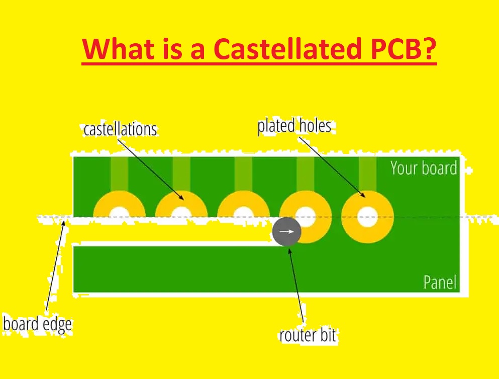
A castellated PCB is a PCB type that comes with small plated half holes over the edges of the board. These half holes are called castellations, providing easy soldering and connection of the board with panels.
Castellation PCB is used in SMT projects, where components are configured on the board surface. It is a commonly used method for PCB assembly.
These boards come with benefits over conventional board designs. The main advantage is the easy assembly process since castellated holes offer easy board soldering points for connecting the board with other components of the board. It helps to reduce the assembly time and also reduces production costs.
Its other benefit is that this board has a compact size since castellated holes exist over the edge of the board and do not take up valuable space on the board.
It provides a compact design and is best for projects where space is limited, like wearable devices or Internet of Things (IoT) products.
Castellation Types
Full Castellations
Full castellations are a type of castellations where the complete edge of the board is notched, making a series of protrusions that are like the castle battlements. This design helps to provide an easy soldering process and make the connection between 2 boards since castellation can easily be soldered directly to pads on mating boards.
This type of castellation is used where board modules are securely connected with mainboards, like wireless communication modules or sensor boards.
Partial Castellations
It is also called half castellations and is like the full castellations but applied to part of the board edge. This structure is used when certain parts of the board need electrical connections or when space constraints restrict the use of full Castellations. It is used where compact power supply modules are connected with a flex board.
Staggered Castellations
Staggered castellations are changes in full or partial castellations design, where notches are offset from one another with the edge of the board.
This design configuration can enhance the mechanical stability of the connection in two boards since a staggered design helps stress easily over the solder joints. It is used in high-vibration conditions and where board connections can face mechanical stress, like in automotive or aerospace electronics.
How Castellated Holes Are Made?
Castellation boards are made with the use of sharp router bits to cut through regular plated holes, leaving half of the hole intact.
These castellations are used for connecting one board to another in signal circuits.
It can be directly soldered on corresponding hole edges on the board, which saves space and reduces the use of any extra connectors.
At the time of the manufacturing process, castellation is made with break tabs that connect the board to a larger panel. The number and position of tabs are based on the size and shape of the board. Normally, castellations are used for regular boards where two out of 4 edges come with special holes.
These castellated holes can be used for replicating certain parts of the board, making the assembly process of completed components with high pin density easy.
For reliable assembly, it is good to use castellated holes having mechanical strength and avoid different problems like delamination.
Use the last online HQDFM Gerber Viewer tool to analyze Gerber files and generate an in-depth Design for
Differences between Simple and Castellated PCB
| Parameters | Simple Board | Castellated PCB |
| Design | Standard Rectangular | Castle Edges |
| Edges and Corners Finishing | Simple and Smooth Finish | Rough Edges on the PCB |
| Soldering | components can Soldered on the Sides of the board | Components soldered on one side only |
| Mounting Methods | Screws, Clips, Adhesive | made to mount PCB onto another PCB |
| Breakout needs | Post-processing of board not needed | Post-processing is for breakout connections |
Castellated PCBs Manufacturing Techniques
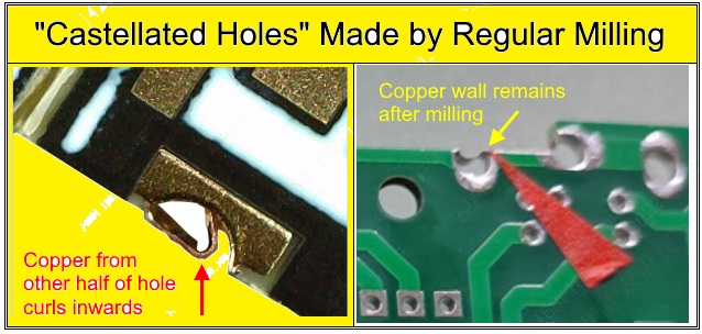
Manufacturing faults in metalized castellated holes, such as copper plating peeling and warping, are issues for the manufacturing process.
Castellated holes Having copper burrs can affect solder connections. It also caused short circuits between neighboring pads for extreme conditions.
Castellated holes are made and plated as standard PTHs are made, but the difficult part is getting the reverse half of every hole out without affecting the first or leaving extra copper.
Here is a detailed process for castellated holes PCB used by JLCPCB explained.
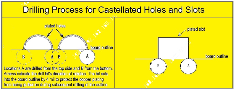
Whether it is drilling or milling, the direction of rotation of the spindle is clockwise. if tools reach point A copper plating on the whole wall moves against the substrate with the tool bit, making sure there is no copper burr, peeling, or residues.
When tools are at point B, there is no support for copper from the hole wall. Since tools rotate forward, their movement results in copper curling in a toll rotation direction, causing copper burrs and residues.
These parameters affect the customer’s installation and use.
JLCPCB is the best-castellated hole process; after drilling and copper plating, they use a step drilling process to ensure that half of the metalized hole is retained.
In other words, the castellated hole is half along the board edge, and making sure the quality of the plating helps users to solder and use it. Now the castellated holes process is properly configured at JLCPCB.
Certain Requirements for Design
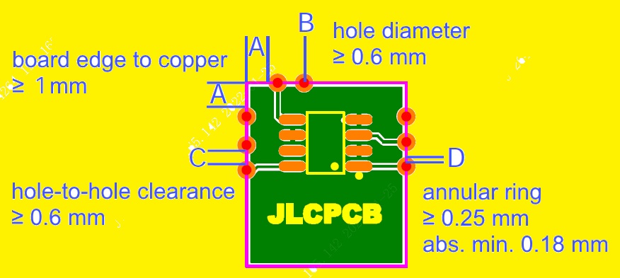
Dimensions
| Dimension | Minimum |
| Board size | 10 mm × 10 mm |
| Board edge to castellated pad (A) | 1.0 mm |
| Castellated pad drill diameter (B) | 0.6 mm |
| Hole-to-hole clearance (C) | 0.6 mm |
| Annular ring (D) | 0.25 mm (absolute minimum 0.18 mm) |
Note: JLCPCB has features to increase annular rings that are less than 0.25 mm in diameter. So provide them remarks with the order if widths less than 0.25 mm exist and select “confirm production files” for modifications.
Pad Shape and Placement
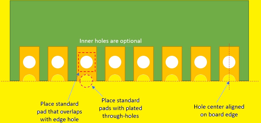
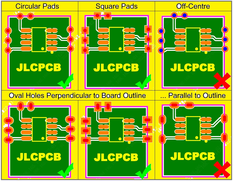
Castellated holes are made round or oval, but give attention to setting the solder pads in the internal part of the board outline.
For designs having 1/3 of holes in the board, seen in Figure 3, this design does not fulfill the demands of the manufacturing process, so holes must be configured on the middle line board outline. With that oval castellated holes parallel to the edge of the board are not processed.
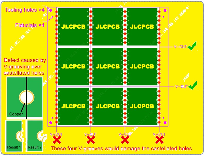
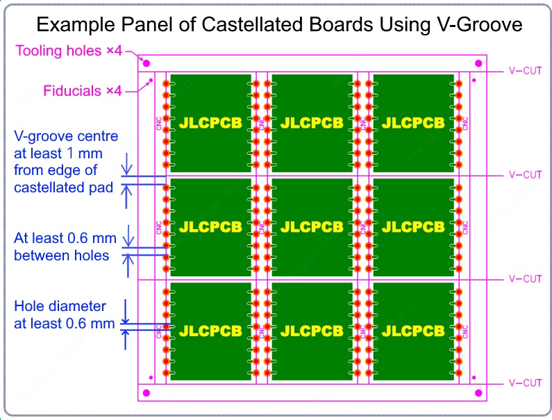
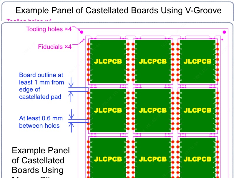
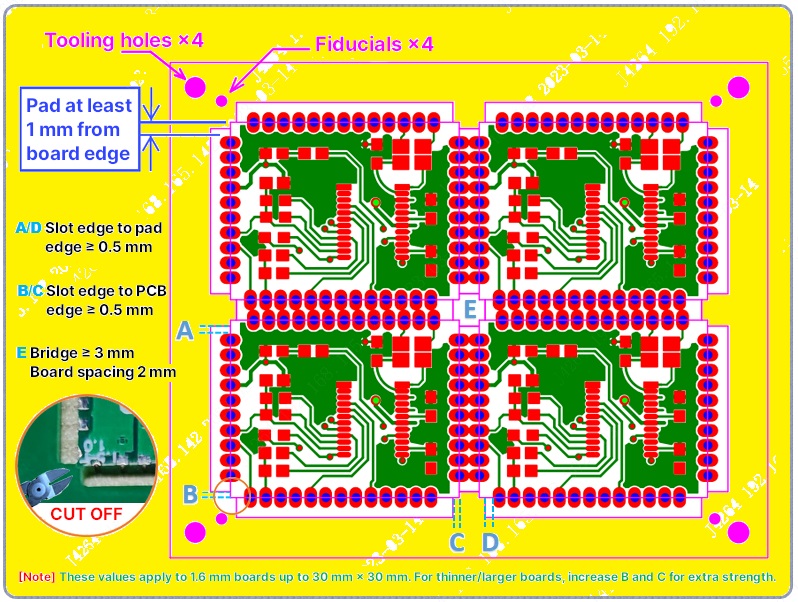
Panelizing Castellated Boards
For castellated boards, single board dimensions can be about ≥ 10 mm, and castellated boards use the V-cut and mouse bite penalization techniques.
So the V-cut shaping is not used on castellated edges; then CNC milling is used for shaping.
V-Cut Panels (Non-Castellated Edges Only)
Mouse Bite Panels
Boards with All Sides Castellated
For high-quality boards, it is important to make PCB design a practical product. The JLSPCB is committed to providing high-quality manufacturing standards with proper use of the latest instruments and getting raw materials from the best suppliers.
With 5 self-owned manufacturing bases, they can make less production costs from larger scale effects on manufacturing.
. Additionally, they give every new member up to $54 in registered coupons. Start purchasing premium PCBs by registering and uploading your Gerber files right now at https://jlcpcb.com.


