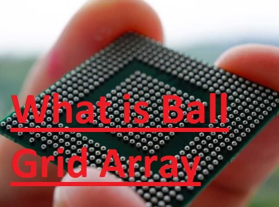
Hi, guys, welcome to the new post. In this post, we will discuss what a ball grid array (BGA) is on a PCB B board. Ball Grid Array (BGA) is a packaging technique used in electronic circuit boards that has different benefits than other packaging techniques. It is used due to its features to handle large interconnections in less area. so used in high-density applications. In this post, we will learn about Ball Grid Array (BGA) and other parameters. So let’s get started. What is a Ball Grid Array (BGA)?
What is BGA?
- BGA integrated circuits are SMD components that do not come with leads. Then they have solder balls that are an array of metallic balls configured on board. Fixing of solder balls of BGA on board is performed through laminated substrate existing at the bottom of the PCB package boards.
- Metallic traces are used for route die connections with solder balls. BGA board packaging provides IO connections, then flat packages and dual in-line boards.
- BGA integrated circuits come with more efficiency and high-speed operation due to short connections from silicon die with solder balls. With the compact lead length and lead space, BGA packages have a good solution for high-speed board devices having densely packed circuits.
BGA vs. Other Packaging Technologies
| Feature | BGA | PGA | LGA |
| Package type | Ball grid array | Pin grid array | Land grid array |
| IC connection | Solder balls | Pins | Solder balls |
| Package size | Compact | Larger | Larger |
| Heat dissipation | Good | Fair | Good |
| Cost | expensive | Less costly | Less costly |
| Complexity | More complicated | Less complicated | Less complicated |
| Applications | High-performance devices, devices with a lot of ICs, thin devices, | , devices that do not need high-performance | devices that do not need high performance |
BGA (Ball Grid Array) Package:
The BGA package is surface mount technology that comes with an array of solder balls on the lower side of the package. These solder balls work as electrical and mechanical connections between the package and the board. BGA packages come with some benefits.
- BGA packages help the high pin count and increase input-output features compared to other packages. So best to use for complex and high-performance applications.
- The solder balls in BGA packages offer good thermal conductivity, helping effective heat dissipation from the board.
- BGA packages provide shorter electrical paths and less inductance and capacitance, resulting in good signal quality and higher-speed electrical performance.
LGA (Land Grid Array) Package:
The LGA package is like BGA, which is surface mount technology. Then having solder balls, LGA packages come with a carry of lands or pads on the lower side that make direct connections with the resulting pads on board. LGA packages have these features.
- LGA packages have lower parasitic inductance and capacitance than BGAs, which are best to use for high-frequency applications.
- The direct contact between packages and PCBs in LGA packages results in good mechanical stability and reliability, specifically for thermal cycling conditions.
Advantages of BGA:
- It has a small size board.
- Less cost
- High efficiency and reliable
- high thermal dissipation
- Best electrical implementation.
Disadvantages of BGA:
- When soldering is finished, inspection is difficult.
- It needed high rework and was highly cautious.
- the high sensitivity of BGA components conditions environmental changes
- It needed electrostatic protection and high storage maintenance.
Features of BGA:
- The board made with this technology needed less space.
- It is a low electrical inductance technique.
- It saves the chip from overheating due to low thermal resistance.
- It has less interconnection density and less board complication due to PoP stacking.
What is a Cold Solder Joint and How Can You Prevent it?
Types of BGA
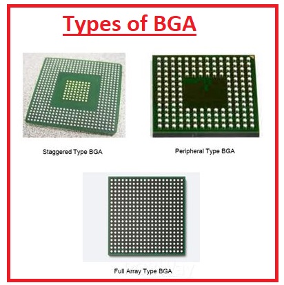
Types of BGA Packages
PBGA:
- Plastic overmolded BGA was created with a plastic-coated casing, a laminated substrate of glass mixture, and etched copper traces. The ball pitch is 1.0 mm, 1.27 mm. 2-4 layered boards of organic matter.
Flip Chip BGA:
- It comes with a multilayer substrate on board.
CBGA:
- Ceramic BGA, where the ceramic substrate is configured with FlipChip (FC) electrical connections.
CDPBGA:
- Cavity Down PBGA comes with a square-shaped low depression in the chip area known as the cavity area.
TBGA:
- This type of BGA comes with a soft-shaped substrate with a one- to two-layer board called Flex Tape BGA.
H-PBGA:
- High thermal BGA.
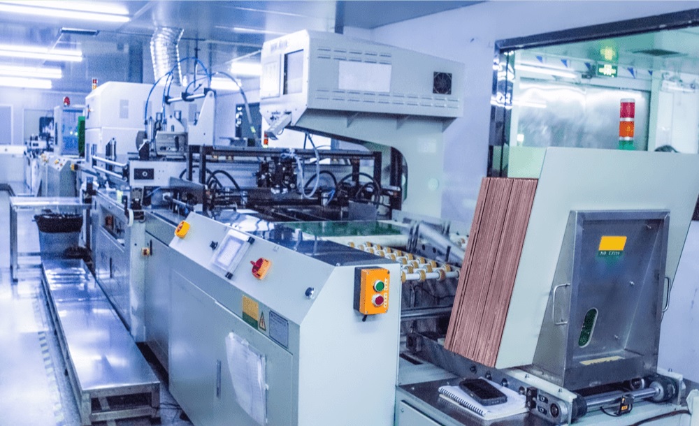
JLCPCB BGA Technology:
As a well-known PCB supplier and services provider, JLCPCB also offers BGA services. The BGA-PCB products are accurately tested at JLCPCB with the use of the proper latest techniques before proving to customers. Their BGA services are according to modern electronic design requirements and make sure different customers’ needs for BGA integration in board design are satisfied with the highest degree of accuracy and quality.
. Here are some of their BGA technology’s salient features:
- Advanced Manufacturing Equipment:
- High-Precision Assembly:
- X-ray Inspection:
- Design Guidelines:
- Quality Assurance: JLCPCB follows the quality guidelines to ensure good performance of BGA assemblies.
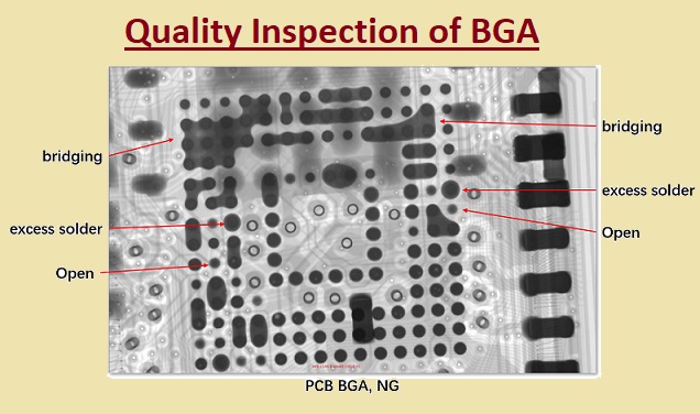
Quality inspection of BGA
The inspection of BGA packages is difficult due to solder ball use. Conventional optical techniques are enough for detecting faults. For increasing accuracy, boundary scan inspection, electrical testing, and X-ray inspection are used in SMT assembly with BGA.
Electrical testing:
- This method finds open circuit and short circuit faults.
Boundary scan inspection:
- Leveraging the inspection port of boundary scan design, this method finds solder-joined boundary connectors to find component opens and shorts.
Automated X-ray inspection:
Automated X-ray inspection checks solder joints with components, showing hidden faults such as voids and bubbles, contrary to AOI, which just checks visible connections. Common BGA defects are loose solder, cold joints, bridge shorts, opens, cavities, missing/dropped solder balls, and irregular sizes.
Elimination of BGA defects:
Detaching of components:
- BGA component defects are solved through disconnecting components on board. This process is performed by heating components of a board that melts solder joints, changes components, and arranges solder connections when required.
BGA rework process:
- This process is performed at a certain part of the factory, and here BGA board components are heated using an infrared heater. The heat level is configured with a thermocouple. The BGA board components are configured by using an infrared heater. The heating level is monitored with the use of a thermocouple. There are vacuum instruments used for lifting the packages on board, and some other instruments are also used.
Localized heating:
- Heating is performed properly and is limited to defective parts of the board. Flow heat for confirming connections of all components on boards
Read also:
- Industrial Control PCB Board
- Types of PCB Board
- Matte vs Glossy in PCBs
- What is PCB Leds Circuit Board: What Do You Need to Know
- Four Layer PCB Layout: Design Process and Cost of Manufacturing
FAQs
What is a BGA in PCB?
BGA, or ball grid array, is a type of surface mount packaging used in integrated circuits. BGA has different techniques for connection and is used for permanently mounting devices. Other packages,, such as quad flat packs, or QFP, used the sides of the package to make connections.
What is the difference between BGA and LGA?
Land grid or LGA packages in a non-socketed configuration do not have balls and use flat contact that is soldered directly to the board.
BGA packages come with balls as their contact in between the IC and board. balls are normally connected with the underside of the IC.
What is the difference between a pin grid array and a ball grid array?
Feature Ball Grid Array (BGA) Pin Grid Array (PGA) Connection type Solder balls Tiny pins Connection arrangement A square grid of rows and columns A square grid of rows and columns Density High Lower Heat dissipation Excellent Good Impedance Low Higher Ease of unsoldering Easy More difficult Deballing Possible Not possible Reballing Possible Not possible Portability High Lower Thermal and mechanical properties Excellent Good Applications CPUs, GPUs, and other high-performance ICs CPUs, other ICs Package variants Many Fewer CPU sockets Many Fewer Cost Higher Lower
What is the difference between PCB and BGA?
The BGA board comes with more interconnection than a normal PCB board, helping the high-density, small-size board. As pins are on the inner side of the board, leads are shorter, resulting in good conductivity and fast operation of the device.
What are the 3 types of PCB?.
- Single-sided PCBs: This board has conductive layers on one side.
- Double-sided PCBs: It has conductive layers on both sides of the boards.
- Multilayer PCs: There are many layers on this board where components can be connected.
What is the function of BGA?
The ball grid array is surface mount packaging used in integrated circuits. BGA packages are used to permanently mount devices like microprocessors.
What is the advantage of BGA?
- It has highly reliable dense pins.
- Good heat conduction
- Low inductance leads to the best electrical performance.
How many types of BGA are there?
Normally it has 3 main types.
Ceramic BGA (CBGA), plastic laminate BGA (PBGA), tape BGA (TBGA)


