 Hello friends, I hope you all are doing great. In today’s tutorial, we will have a look at MOSFET Bias Circuits. The MOSFET is type of FET and stands for metal oxide field effect transistor used as amplifier and switch in different circuit configurations. In digital and analog circuits MOSFET is commonly used than BJT. There are 2 further main types of MOSFET: E-MOSFET and D-MOSFET.
The main benefit that it provides over the BJT is that it needs a very less amount of current at the input for controlling of a load. In today’s post, we will have a detailed look at its different basing methods and their related circuits with the detailed. So let’s get started with MOSFET Biasing Circuits.
Mosfet biasing Circuits
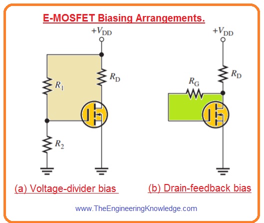
E-MOSFET Bias Configuration
- Since for E-MOSFET the value of VGS should be larger than the threshold value VGS(th), so zero biasing cannot be used.
- In below figure you can see 2 configurations of E-MOSFET biasing.
- In these configurations n channels, MOSFET is used.
- Two biasing configurations are shown first is voltage divider and second one drain feedback bias.
- The benefit of the use of this 2 configurations is to make more positive at the gate than by the source through the amount VGS(th).
- The equation for voltage divider bias configuration is given here.
VGS=[R2/(R1 + R2)]VDD
VDS=VDD – IDRD
- In this equation ID will be equal to K(VGS – VGS(th))2we have discussed this expression in last tutorial about MOSFET.
- In drain feedback bias circuitry shown in figure the gate current is very less and so there will be no voltage drop about the resistance RG. So VGS = VDS.
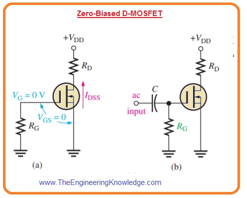
D-MOSFET Bias Configuration
- As we know D-MOSFET can operate with both positive and negative values of VGS voltage.
- The basic method of biasing is to make VGS=0 so ac voltage at gate changes the gate to source voltage over this zero voltage biasing point.
- Zero bais configuration for MOSFET is shown in below figure.
- As VGS is zero and ID=IDSS as denoted. The drain to source voltage will be.
VDS = VDD – IDSSRD
- The main function of RG is to sustain an ac voltage input by separating it from the ground as shown in figure denoted as b.
- As there is no dc gate current there will be no effect of RG on zero gate-to-source bias.
How to bias a MOSFET
- For biasing of MOSFET is voltage given at the source and gate pins of this transistor. The connected voltage on the MOSFET helps the current to move the drain towards to source. Current flow based on gate voltage and MOSFET structure
Mosfet biasing circuits are
- Fixed bias:
- In this biasing technique, a voltage supply is given to the gate and source. It is a less stable type of biasing and simply considered
- Voltage divider bias:
- In this circuit reference voltage is produced with the creation of a voltage divider. The gate pin of MOSFET is connected with a reference voltage. It is a complicated structure but considered as fix
- Self-bias:
- It produces its bias voltage.
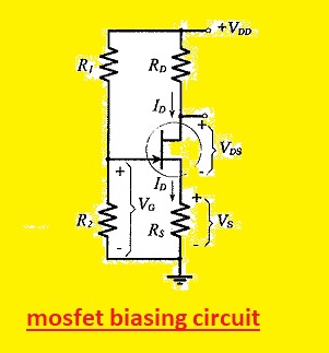
mosfet biasing circuit
Why do we need to bias a MOSFET?
- MOSFET enters in cutoff region and the result is a distortion signal. To avoid it there is need to bias MOSFET like DC drain voltage is small as possible.
What are the biasing regions of a MOSFET?
- The MOSFET comes with 3 different regions of operations. These regions are called the Ohmic/Triode region, Saturation/Linear region, and Pinch-off point.
What is MOSFET drain bias?
- For high drain biases, channel carriers gain enough energy to cause impact ionization. Fo N channel MOS, holes come out of body terminals through SI resistance and make positive voltage losses over the body and source junction.
What is a biased circuit?
- Biasing is defined as fixed dc voltage or current provided to terminals of electronic components like diode transistors or vacuum tubes in circuit where ac signals exist, for making accurate operating conditions of components.
Why is MOSFET reverse biased?
- Reverse bias reduces run-off time as the gate works like capacitance and reverse biased removes charge faster.
What is the working principle of a MOSFET?
- If voltage is provided to the gate, an electrical field is produced that changes the width of the channel region where electrons move. The larger channel region will have good conductivity.
Does MOSFET drain positive or negative?
- Source and drain terminals based on the polarity of voltage connected with it. For N channel, the drain is more positive. for p channel drain is the negative terminal
What is the Q point of a MOSFET?
- The Q point is the operating point of the amplifier where not signal is provided. it defines voltage and current levels over MOSFET and the load resistor and affects the gain, distortion, and output range of amplifiers.
What is called biasing?
So friends that is a detailed post about the MOSFET Bias if you have any questions ask in the comments. Thanks for reading