 Hello dear students, I hope you all are doing great. In today’s tutorial, we will have a look at Introduction to BJT (Bipolar Junction Transistor). The transistor was created in by J.Barden, W Shockley and W. Bratterin in 1947. A transistor name was given to this component by John R.Pierce. At the time of creation, it is known as a solid-state type of vacuum triode but knows known as a transistor. It is an electronic component mainly used for amplification and switching purposes.
As the name suggests, it is composed of two junctions called emitter-base junction and collector-base junction. In today’s post, we will have a detailed look at BJT (Bipolar Junction Transistor) working, construction, and some related parameters. So let’s get started with Introduction to BJT (Bipolar Junction Transistor).
Introduction to BJT (Bipolar Junction Transistor)
- The BJT stands for bipolar junction transistor is an electronic device that has 3 terminals and used in different amplification circuits. It also known as current controlling instruments.
- Its 3 terminals are emitter, base, and collector, also have two pn junctions.
- The junction formed through the base and emitter called base-emitter junction and combination of base and collector makes the base-collector junction.
- There are 2 further types of BJT first is NPN and the second one is PNP. These types are designed according to doping level.
- As it used in for amplification process for this it needed an external dc source,
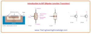
- In below figure the symbol and internal structure of BJT are shown below.
BJT Working
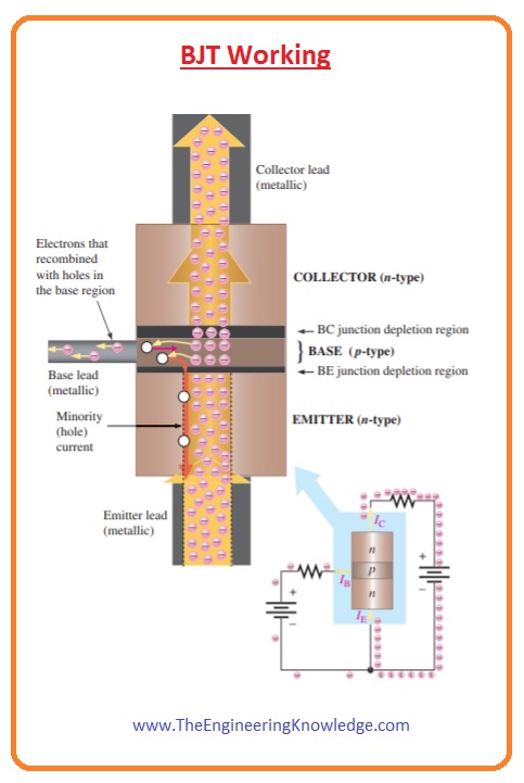
- For an understanding of the working of BJT transistor lets discuss the internal structure of NPN transistor.
- In the below figure you can see that the emitter part which is n-type of a transistor is highly doped and has a large number of free electrons.
- Free electrons of n region will enter into the base which is P-type and has less area, through the forward-biased base-emitter junction. It represents in a figure through a wide arrow.
- The base of the transistor has less number of holes that are also majority carriers shown through white color circles.
- Some electrons entered in the base region combine with the holes and move like valence electrons in base and in emitter as hole current shown in a figure through red color arrows.
- The electrons combined with the hole exits from the structure of base they move like free electrons in the metal base lead and generates an exterior base current.
- Due to less area of base mostly electrons entered int the base do not combine with the holes.
- When electrons moves towards the base-collector junction which is in the reverse biased condition these electrons move to the collector due to the positive voltage across the collector.
- Electrons entered the collector region in the exterior circuit and after this enter in the emitter of a transistor with the base current as represented in the figure.
- The emitter current is somewhat larger than the collector current since of the less base current that divides from the total current entered into the base region from the emitter
BJT Currents
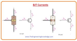
- In the below figure for both NPN and PNP transistors, the current direction and symbol are shown.
- The arrow on the emitter of transistor indicates the direction of conventional current.
- In figures of both NPN and PNP transistors, you can see that emitter current is equal to the base and collector current.
IE =IC + IB
- IB is less as compared to the emitter and collector current.
BJT Characteristics And Parameters
- There are 2 main parameter that describes the characteristics of BJT first one is βDC which called dc current gain and αDC.
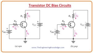
- In the below figure the transistor is connected with a dc bias and both NPN and PNP configuration is shown.
- In this circuit base-emitter junction is forward biased through the VBB and base-collector junction is reverse biased through the Vcc.
DC Beta (βDC) and DC Alpha (βDC)
- The dc current gain of transistor is the ratio between dc collector and dc base current. It denoted as (βDC).
(βDC)= IC /IB
- Normally the value of dc current gain is from less than twenty to two hundred or greater.
- On the datasheet of a transistor (βDC) is denoted as equivalent hybrid (h) factor, hFE.
hFE = βDC
- The ratio between dc collector and dc emitter current is known as dc alpha or (αDC).
- Normally beta is largely used in transistor circuits as compared to alpha.
aDC = IC/IE
- usually, the value of aDC is from 0.95 to 0.99 or larger but it remains always less than one.
- It is less than one due to the value of the collector current is less than the emitter current.
BJT DC Model
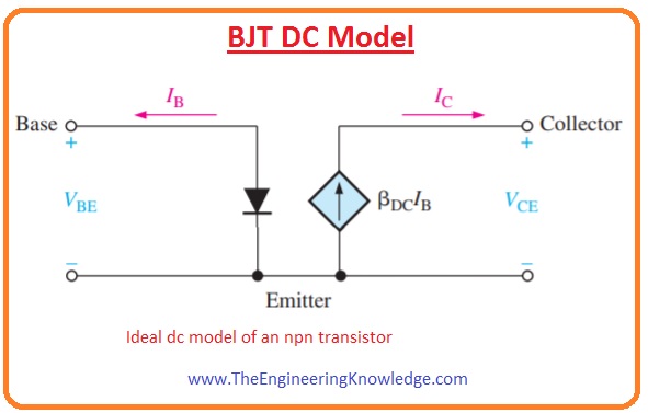
- In the below figure you can see the circuit arrangement for NPN transistor which shows the unsaturated bipolar junction transistor as a module with current input and dependent current source as output.
- Input circuit diode in the forward biased condition through which base current is flowing.
- The output is a dependent current source whose shape is similar to the diamond has a value that depends on the base current IB at the input and equal to the βDCIB.
BJT Circuit Analysis
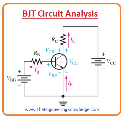
- In below figure you can see the basic bias circuitry arrangement of transistor.
- IE is the dc emitter current.
- IC is the dc collector current.
- VBE is the value of the voltage at base with respect to the emitter.
- VCB is value of voltage at collector with respect to the base.
- VCE is the value of dc voltage at collector with respect to emitter.
- In above circuitry, the base-emitter junction is in forward biased condition due through VBB and base-collector junction is reverse biased condition through the VCC.
- Base emitter junction during forward biasing condition it behaves like a diode in forward biased condition and has a value of voltage drop across it 0.7 volts.
VBE=0.7
- In real transistor the value of VBE can be 0.9 volts and depend on the current.
- If we apply KVL on above circuit than we will have the value of RB
VRB = VBB – VBE——(1)
- According to Ohm’s law.
VRB = IBRB
- If we put the value of VRB in above equation than we have.
IBRB = VBB – VBE
- For value of base current we simiply it.
IB= (VBB-VBE)/ RB
- The value at collector with respect to the grounded emitter is given as.
VCE = VCC – VRC
- The value of voltage loss about RC is given here.
VRC = ICRC
- The value of collector with respect emitter is.
VCE= VCC-ICRC
- In above equation Ic is βDCIB
- The voltage at the collector-base junction is given here.
VCB = VCE – VBE
BJT Collector Characteristic Curves
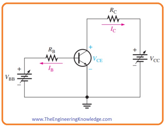
- By using below circuit the collector characteristic curve can be created that explains the about variation in collector current with the changing in collector to emitter voltage VCE for certain value of base current.
- You can also see that VBB and VCC are variable voltage sources.add pic bjt circuit
- Suppose that the value of VBB is such that base current IB and Vcc are zero.
- During this condition, the base-emitter and base-collector junction are at forward biased conditions since the base voltage is almost 0.7 volts and voltage at emitter and collector is zero.
- The IB is flowing through the base-emitter junction since the less resistive path to the ground and collector current is 0.
- If both junctions of a transistor are in forward biased condition than the transistor is in the saturation region.
- It is a condition of a transistor at which the collector current has its extreme value and does not depend on the base current.
- With the increment in Vcc, VCE increase with the increment of collector current.
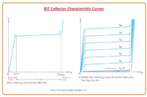
- It shown in curve denoted (b) in below figure among point A and B.collector current increases due to increment in Vcc since VCE has value less than the 0.7 volts due to the forward biased collector junction.
- In ideal case when the VCE is larger than the 0.7 volts, then base-collector junction is in reversed biased condition and diode now operating in the active region.
- When base-collector junction is in reverse biased condition collector current levels off and has a constant value for a specific value of base current while VCE is continuously increasing.
- Actually, IC upsurges very less as VCE surges due to the broadening of the base-collector depletion region.
- It causes the less hole combination in base due to that there is an increment in βDC.
- It is represented in curve b between points B and C.
- In this part of curve the characteristic curve collector current can be fined by this expression. IC= βDCIB
- If VCE has very high value the reverse-biased base-collector junction now in in the breakdown and Ic increases very fast as shown at right side of point C of curve denoted (b).
- The diode does not operate in this breakdown region.
- A family of collector characteristic curves is formed when IC vs VCE is designed for numerous values of IB, as demonstrated in Figure (c).
- When IB is 0, the transistor is in the cutoff region though there is a very less collector leakage current as shown.
- Cutoff is known as the nonconducting condition of a transistor. The amount of collector leakage current for IB zero is inflated on the graph for an explanation.
BJT cutoff Region
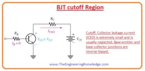
- As we discussed above that when base current is zero than transistor is operating in the cutoff region. It shows in below figure
- In this circuit base, connections are open which results in the zero value of base current.
- In this state, there is very less value of collector current ICEO flow due to carriers generated through thermally.As value of ICEO is very less so it will be ignored for circuit analysis so that VCE = VCC.
- Both base emitter and base-collector junction are not forward biased condition in cutoff region.
BJT Saturation
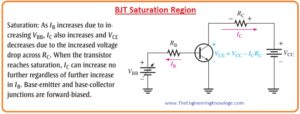
- When a base-emitter junction is in forward biased condition the IB increases the value of Ic also increases according to this equation (IC =βDCIB) while VCE decreases due to increment in collector current according to this equation VCE =VCC – ICRC. It is explained in the below figure.
- When the value of VCE is saturated the base-collector junction is in forward biased condition and Ic will not increases further with the increment in base current.
- At saturation, the equation IC=βDCIB is not valid. VCE(sat) for a transistor exits point lower the knee of the collector curves, and it is generally only a few 10th of a volt.
BJT DC Load Line
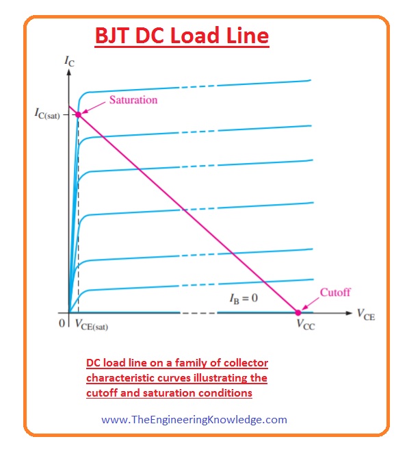
- Cutoff and saturation can be described relating to the characteristic curve with the use of load line.
- The below figure shows the dc load line created on the group of curves connecting the cutoff point and saturation point.
- The lowest of the load line is at ideal cutoff where IC = 0 and VCE =VCC. The topmost of the load line is at a saturation point where IC = IC(sat) and VCE = VCE(sat).
- Between cutoff and saturation of load line, there is an active region of transistor working.
More About βDC
- βDC is a very important factor of bipolar junction transistor so we must know something more about it.
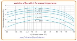
- It is not a constant parameter its value changes with the variation in temperature and collector current.
- By putting the temperature of junction constant and enhancing the collector current increase the value of βDC to an extreme point.
- A more increment in collector current beyond this extreme point decreases βDC.
- If the value of collector current is constant and changes the current value βDC varies in direct relation with the temperature.
- If temperature increases βDC
- In below figure relation βDC with collector current and junction temperature is shown for BJT.
- Add pic
- At datasheet of the transistor shows the βDC at specific values of collector current.
- For the same value of Ic and temperature βDC has a different value for different type of transistors due to the variation manufacturing process.
BJT Maximum Transistor Ratings
- Like other electronic instruments, there are some limitations to bipolar junction transistors.
- These restrictions are defined in the shape of extreme ratings and usually on the datasheet of devices.
- Usually, maximum ratings of BJT are given in the form of VCB, VCE, VEB, Ic and power dissipation.
- The multiple of VCE and Ic should be less than the maximum power dissipation.
- The value of both VCE and Ic cannot be extreme at the same time.
- if VCE is maximum than collector current can be fined as.
Ic= PD(max)/VCE
- If the value of the collector current is maximum than the VCE can be fined by this equation.
VCE = PD(max)/Ic
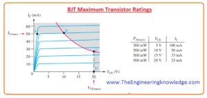
- For BJT the curve for max power dissipation can be drawn on the collector characteristic curve as shown in the below figure.
- These calculations are also mentioned in the form of a table.
- Suppose that PD(max) is five hundred milliwatts, VCE(max) is twenty volts and IC(max) is fifty milliamperes.
- The curve displays that this specific transistor cannot be functioned in the shaded part of the graph.
BJT Derating PD(max)
- PD(max) is frequently stated at twenty-five centigrade. For larger temperatures, PD(max) value is small.
- Datasheet of BJT usually shows the derating factor for calculation of PD(max) at a temperature of over twenty-five celsius.
- For instance, the derating factor of two milliwatts per Celsius shows that max power dissipation decreased to two milliwatts for every degree Celsius increases in temperature
BJT Datasheet
- In the below figure the datasheet of 2N3904 NPN transistor is shown.
- You can see that the value of extreme VCEO is forty volts.
So, friends, it is a detailed post about BJT I have explained each and every parameter related to BJT in this post. If you have any question ask in comments, thanks for reading,





The Introduction to BJT (Bipolar Junction Transistor) article is one of the best I
have ever read!
thanks