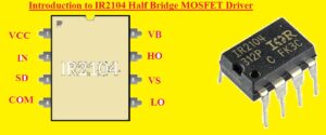
 Hello, readers welcome to the new post. Today we will discuss Introduction to IR2104 Half Bridge MOSFET Driver. It is a high voltage high-speed MOSFET and IGBT driver. It has high dependent high and low side reference output channels. Proprietary HVIC Immune Latch CMOS technology enables durability
monolithic construction. The logic input has compatibility with standard CMOS or LSTTL, output up to 3.3V logic.
The output converters have a high pulse current equalization stage designed for minimal converter crossover. The floating channel can be employed to drive an N-channel power MOSFET or IGBT in a high-side configuration that functions from 10 to 600 volts. In this post, we will discuss the IR2104 Half Bridge MOSFET Driver working pinout and some related parameters. So let’s get started
Introduction to IR2104 Half Bridge MOSFET Driver
- The IR2104 is a half-bridge driver that gets low power input to output a high current driver. It provides the gate high power transistor similar to the power MOSFET.
- With that IR2104 gate driver works as the level shifter and power amplifier
- The IGBT and MOSFET driver output channels operate on high and low side references. The logic input operates on 3.3 volts of logic and has compatibility with LSTTL and CMOS output.
- These methods are immune to proprietary HVC and latch. So it permits monolithic construction
IR2104 Half Bridge MOSFET Driver Features
- Some features of IR2104 Half Bridge MOSFET are discussed here
- It has a match propagation delay for two channels
- It shut down input off both channels
- There is in phase configuration to the high side of output to input
- It has deadtime adjusted innerly
- It has cross-conduction prevention logic
- It has compatibility with 3.3 volts, five volts, and fifteen volts
- It has an Undervoltage lockout
- Its gate drive supply range is about ten to twenty volts
- dV/dt immune
- It has tolerance to negative transient voltage
- It has complete operational to plus six hundred volts
- Its floating channel has compatibility with the bootstrap operation.
| Features | Details |
| input signals | 3.3V-15V |
| Fully operational | 600V |
| Gate drive supply range | 10 to 20V |
| Operating Temperature | -40°C~150°C TJ |
| Pinout | SMD-based design |
| Package | 8-DIP |
| Average load current | 10amps |
| Peak current | 20amps |
| VCC voltage range | 12V to 36V DC |
| Logic gate voltage supply | 12-15V DC |
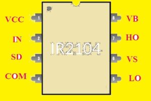
IR2104 Half Bridge MOSFET Driver Pinout
- It has eight pinouts that are discussed here
- VCC is logic and internal gate driver supply pin
- IN is the input pinout
- SD is shutdown or active low
- COM is chip power and signal ground
- LO is low side gate driver output pinout
- VS is high side floating supply retund terminal
- HO is high side gate driver output pin
- VB is high side gate driver floating supply

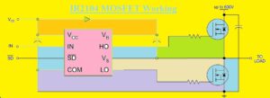
IR2104 MOSFET Working
- The circuit diagram of the IR2104 gate driver’s working operation is shown here.
- It is noticeable that bootstrap diode and bootstrap capacitors are used for high-side driving the module. The value of the bootstrapping capacitor has an impact on high-side switching.

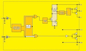
IR2104 MOSFET Block Diagram
- In below figure IR2104 block diagram is shown

IR2104 Operating Conditions
| Parameter | Minimum | Highest |
| High side floating supply absolute voltage | VS + 10 | VS + 20 |
| High side floating supply offset voltage | Note 1 | 600 |
| High side floating output voltage | VS | VB |
| Low side and logic fixed supply voltage | 10 | 20 |
| Low side output voltage | 0 | VCC |
| Logic input voltage (IN & SD) | 0 | VCC |
| Ambient temperature | -40 | 125 C |
Equivalents for IR2104
• DGD2104
• IR2103
• IRS2104
• IR2153
• IR2110
IR2104 MOSFET Applications
- Its main applications are discussed here
- It used in robots
- Used in inverter circuits
- It used in switch-mode power supply circuits
- Used in power instruments
- Motor driver circuits have these components
IR2104 vs IR2101
| Features | IR2104 | IR2101 |
| Package | SOIC-8 | DIP-8 |
| Driver | 600V 2-OUT | High and Low Side |
Logic input compatible | Standard CMOS or LSTTL | – |
Frequently Asked Questions
How does IR2104 work?
- The integrated circuit IR2104 is a half-bridge MOSFET gate driver. It is used for operating the high and low sides of the MOSFET with the use of a PWM signal with Arduino Pin D9. The module also controls through a control signal with Arduino Pin 3. It has a PWM duty cycle of 99.9 percent for keeping the charging pump operating.
What is a half-bridge gate driver?
- The isolated half-bridge driver operation is to operate gates of the high and low sides of the N-channel MOSFET with low output impedance for reducing conduction losses and high-speed switching time for minimizing the switching losses.
What is the difference between a half-bridge and a full-bridge inverter?
- The basic difference is that the output voltage for a full bridge inverter is equal to the power supply voltage, and the output voltage for a half bridge inverter is equal to one half of the power source voltage.
What is the difference between IRS2104 and IR2104?
- The IRS2104 comes with a higher speed rise and fall than the thanIR2104.
Why is the IR2104 MOSFET driver not working?
- For chip enabling, set the SD pin to a high level. If you are activating the SD pin, there is a need to use a base resistor. Without the BSE resistor, the input is not higher than 0.7 volts, which is unlikely for activating theIR2104.
That is all about the IR2104 all details has explained. If you have any queries ask here. As this module has an amplifier and level shifter configuration IC operates low-power input from the microcontroller to generate high curent. This characteristic of this module helps to use it in different circuits like DC brushed motors, industrial drivers induction coil drivers


