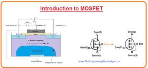
 Hello friends, I hope you all are doing great. In today’s tutorial, we will have a look at Introduction to MOSFET. The MOSFET is stands for metal oxide semiconductor field effect transistor is a type of field-effect transistor like the JFET. As we know that in JFET pn junction is exits but in MOSFET it, not exits. In place of its gate of MOSFET is separated from the channel by the layer of silicon dioxide. There are 2 main types of MOSFET first one is an enhancement and the second one is depletion denoted as D.
The most commonly used MOSFET is enhancement. Since in place of metal for gate polycrystalline silicon is used. These electronic components is known as IGFET or insulated gate FET. In today’s post, we will have a detailed look at its working, application, types and some related factors. So let’s get started with Introduction to MOSFET.
Introduction to MOSFET
- The MOSFET is also known as metal oxide silicon transistor or MOS is a category of IGFET or insulated gate FET which is manufactured with the thermal oxidation of semiconductor material usually silicon.
- The voltage of the insulated gate calculates the electrical conductivity of the transistor this behavior of variations in conductivity with quantity if given voltage can be used in amplifier and switching circuits.
- In 1959 first time MOSFET was created by the Egyptian engineer Mohamed M.Atalla and Dawon Kahng who was Korian engineer.
- This electronic component is most commonly used in electronic circuits and from 1960 to 2018 almost (1.3 × 10²²) MOSFETs have been created.
- It also used very commonly in digital, analog circuits and power instruments.
- The main benefits of MOSFET are that there is no need for input current to regulate load current is it required in BJT.
- The voltage given to the gate of E-MOSFET can increase the conductivity from off condition.
- While for D-MOSFET voltage given at gate can decrease the conductivity from on condition.
- The switching speed of this module is high, their size is small, uses less amount of power.
E-MOSFET (Enhancement MOSFET) Transistor
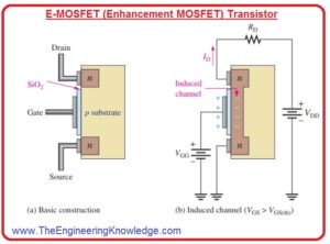
- The enhancement MOSFET functions only in the enhancement mode and there is no depletion-mode exits in it.
- The main difference between E-MOSFET and D-MOSFET is that in E MOSFET there is no structural channel.
- In below figure denoted as you can see that substrate has expands to the layer of silicon dioxide.
- For n channel MOSFET the positive voltage at the gate over threshold value induces a channel by making a thin region of negative charges in substrate close to the silicon dioxide layer as shown in above figure denoted that ‘b’
- The conductive behavior of the channel increases with the increment in gate to source voltage that causes movement of electrons toward the channel region.
- The value of voltage less than threshold there is no channel exits.
E-MOSFET Symbol
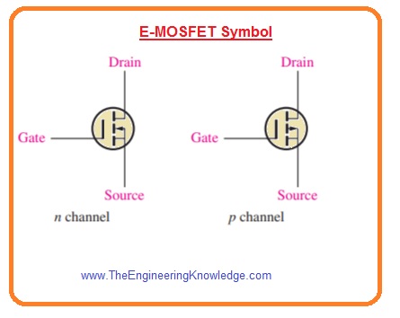
- In below figure you can see the symbols for N and P channels E-MOSFET are shown.
- The dashes indicate that the physical channel does not exist.
- The inward substrate arrow indicates n channel and outward direction arrow show p channel.
Depletion MOSFET (D-MOSFET)
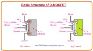
- The second type of MOSFET is D MOSFET its structure is shown in below figure.
- In this structure drain and source are diffuse with the substrate substance and than linked with the small area channel close to the insulated gate terminal.
- Both N and P channel D-MOSFET are shown in above figure.
- To understand of basic operation, we discuss the N channel D-MOSFET the working of P channel is also similar to the different voltage polarities.
- There are 2 operating modes of D MOSFET first is depletion mode and second is enhancement mode so it is also known as depletion/enhancement MOSFET.
- As there is insulation among gate and channel so positive or negative voltage can be provided.
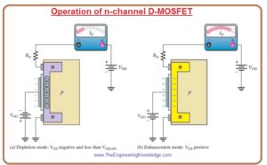
- The n channel MOSFET functions in depletion mode when we provide negative voltage to the gate to source and operate in enhancement mode when gate to source voltage is given.
- Normally it operates in depletion mode of operation.
Depletion Mode
- We consider the gate as first plate of the capacitor and the channel as the second plate.
- the insulating layer of silicon dioxide is the insulating material between them.
- Through Negative voltage at the gate conduction electrons bear the force of repulsion due to negative charges and positive ions are formed at their place.
- So electrons of N channel decrease that reducing the conductivity of the channel.
- The larger the negative voltage on the gate the increases the reduction of N channel electrons.
- At highly gate, to source voltage or VGS(off) the channel is completely depleted and the value of drain current is 0.
- In below figure denoted as ‘a’ depletion mode is explained.
- similar to the JFET the n channel D-MOSFET operates drain current for gate-to-source voltages among VGS(off) and 0.
- The D-MOSFET operates for values of VGS over 0.
Enhancement Mode
- Due to positive voltage across gate electrons moves toward the channel that increases the conductivity of channel it is explained in above figure denoted as ‘b’.
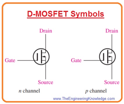
D-MOSFET Symbols
- The symbolic representation for both N and P channel D-MOSFET are shown in below figure.
Structures of Power MOSFET
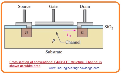
- The channel is longer of the conventional E-MOSFET it shown in below figure.
- This causes a large drain to source resistance and due to this enhancement MOSFET is used only for less power applications.
- When the gate is positive the channel is created close to the gate between the source and drain as shown in the above figure.
Laterally Diffused MOSFET
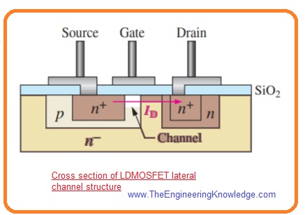
- The structure of LDMOSFET or Laterally Diffused MOSFET has a lateral channel structure and it is a category of E-MOSFET created for power applications.
- The channel of this module is small among the drain and source than normal E-MOSFET.
- Due to small channel, resistance is less that causing high voltage and current to flow.
- In below figure the internal structure of LDMOSFET is shown. When a gate is small n channel induces in the P layer among the less doped source and n-region.
- The current among drain and source through the n regions induced channel is shown in the figure.
VMOSFET
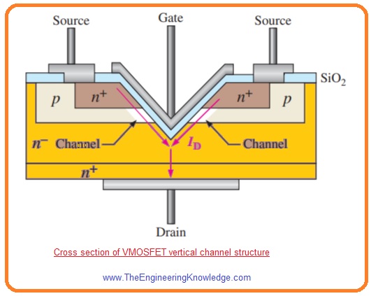
- The VMOSFET or V-groove MOSFET is another type of conventional E-MOSFET created to get large power capability by making a small and wide channel with less resistance among drain and source with the use of vertical channel structure.
- The small and wide channels are best for large current high power dissipation.
- It also increases the frequency response.
- There are 2 source connections on VMOSFET first is gate connection on upper part and the second is drain connection at the lowest part is shown in the below figure.
- The channel is induced at an angle of ninety degree along both sides of the V-shaped groove among the drain and the source connections.
- The length of channel is specified by the thickness of layers that is regulated by the doping intensity and time used for diffusion than by the dimensions of mask.
TMOSFET
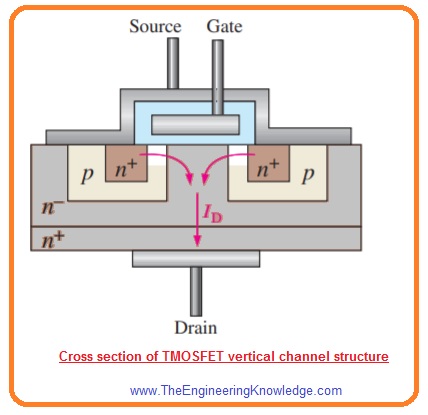
- In below figure vertical channel structure of TMOSFET is explained.
- The gate structure is entrenched in a silicon dioxide layer, and the source interaction is constant over the complete surface area.
- The drain is at the lowest part TMOSFET attains larger packing compactness than VMOSFET, though have the short vertical channel benefit
Dual-Gate MOSFETs
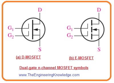
- The category of dual gate MOSFET can be either enhancement or depletion.
- The main difference is that it has 2 stage as shown in below figure.
- The one disadvantage of the field effect transistor is that its input capacitance is large which limits it use in large frequency applications.
- The use of dual gate MOSFET decreases input capacitance so it is beneficial in high frequency RF amplifier circuits.
- Other benefit of dual gate configuration is that it provides an automatic gain control input in radio frequency amplifiers.
MOSFET Characteristic
E-MOSFET Transfer Characteristic
- In Enhancement MOSFET there is use of enhancement channel only. So n channel MOSFET needs a positive gate to source and p channel MOSFET needs a negative gate to source voltage.
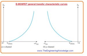
- In the below figure you can see the characteristic curve of both types of Enhancement MOSFET.
- You can note that there is no drain current when VGS=0. So there is no IDSS factor for E-MOSFET as JFET and D-MOSFET have.
- You can note that there is nor drain current exits till VGS get a specific nonzero value known as threshold voltage, VGS(th).
- The equation of transfer characteristic curve of enhancement MOSFET changes from the JFET and Depletion MOSFET since curve begins at VGS(th) than
VGS(off) on X-axis never crosses the y-axis. - The mathematical expression for E-MOSFET transfer characteristic curve is given as.
ID =K(VGS VGS(th))2
- In this equation K is constant and its value depends on the specific MOSFET and can be find from the datasheet through value of the current ID which is known ID(on).
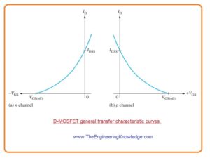
D-MOSFET Transfer Characteristic Curve
- As we discussed that D-MOSFET can function with positive or negative gate voltage.
- It is mentioned on the general transfer characteristic curve in below figure.
MOSFET Handling Precautions
- All types of MOS components can damaged from electrostatic discharge.
- Since the insulation among the MOSFET gate and channel due to that input Resistance is large.
- The leakage current IGSS has a range of pA for typical MOSFET while the reverse current for JFET is in the range of nA.
- The input capacitance outcomes from the insulated gate structure.
- A large amount of excess static charge can be stored since input capacitance combines with very large value of input Resistance to damage the component.
- To stop the cause of damage from ESD there are some steps you should follow to when use MOSFET.
- Very carefully remove MOSFET from their packing. They are transported in conductive foam or special foil conductive casing. Generally, they are dispatched with a wire ring about the terminals, which is detached when MOSFET is used in any circuitry.
- All tools and metallic benches used in assemblage or testing must be linked to the earth ground.
- The wrist of the user must be attached with the grounding band that has large value series resistacne for protection. The resistor stops unintentional interaction with voltage from becoming fatal.
- When power is on no remove MOSFET from the circuitry.
- When DC power supply is not given do’nt give a signal to MOS components.
So friends that is a detailed post about MOSFET if you have any questions ask in comments. thanks for reading. Have a good day.



This site was… how do I say it? Relevant!! Finally I’ve found something that helped me. Appreciate it!