 Hello friends, I hope you all are doing great. In today’s tutorial, we will have a look at Common-Drain FET Amplifiers. The common drain amplifier configuration is associated to the common collector amplifier configuration of BJT. We can also say that the common amplifier which we discussed in the previous tutorial is the follower of common emitter amplifier configuration. This common drain is a follower of the source amplifier that we discussed in the last tutorial.
In this configuration value of the voltage at the source is similar to the input or gate voltage and has also the same phase. In simple words source, voltage is a follower of input voltage at gate. In today’s post, we will have a detailed look at its circuit, working, and some related parameters. So let’s get started with Common-Drain FET Amplifiers.
Common-Drain FET Amplifiers
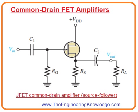
- The common drain junction field effect transistor amplifier is such an amplifier in which input is given to the gate and output is taken out from the source to make drain terminal common for both gate and source.
- As drain is common so there is no need of drain resistance. In below figure you can see the common drain JFET amplifier configuration.
- The common drain configuration is also known as source follower.
- In this circuitry, self-biasing is used. The input voltage is given to the gate with the use of a bypass capacitor denoted as C1 and output is coupled with the load resistance through capacitor C2.
Common-Drain FET Voltage Gain
- Like another amplifier for this amplifier configuration, the voltage gain is Av=Vout/Vin.
- For source follower configuration Vout is
IdRs and Vin is Vgs +IdRs it shown in the below figure.
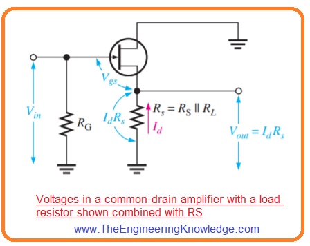
- So gate to source voltage gain will be IdRs/(Vgs +IdRs).
- Putting Id =gmVgs into above equation we have the resultant expression as.
Av=gmVgsRs/(Vgs + gmVgsRs)
- So we have.
Av=gmRs/(1+gmRs)
- Note that the gain value is always less than one. If gmRs>>1 the good approximation is Av=1.
Common-Drain FET Input Resistance
- Since input voltage is given to the gate the input resistance observed by the input signal source is very large like a common source amplifier.
- The gate resistance RG is in parallel with the input resistance observing at the gate the total input resistance will be.
Rin=RGΙΙRIN(gate)
- Here RIN(gate) = VGS/IGSS.
So friends that is a detailed post about Common-Drain FET Amplifiers if you have any queries ask in the comments. Thanks for reading. Have a good day.
What is Common Drain Amplifier

- Common drain amplifiers also called source followers and belong to normally used 3 single-stage field effect transistor configurations and are used as a voltage buffer.
- In this configuration gate terminals of transistors work as signal input, source output, and drain is common for both input and output.
- Due to the low impedance of the load resistor on voltage gain, it is used to operate low resistance load like a speaker.
- The BJT transistor circuit is a common collector amplifier. This circuit is known as a stabilizer.
- With that circuit used for transforming impedances, such as the Thevenin resistance of the combination of voltage followers operating with a voltage supply with high Thevenin resistance is decreased to the output resistance of the voltage of followers.
- That reduction in resistance makes a combination of ideal sources.
- The voltage follower added between the driving stage and high load, provides infinite resistance to the driving phase, the benefit for coupling voltage signal to heavy load
Applications of common drain amplifiers:
The common drain or source follower circuit has featues to provide high input impedance and low output impedance and is used to work as a buffer amplifier. According to input and output impedances, the output voltage can be sampled and used input in series with input voltage.
Read also:
- Difference between Thyristor and MOSFET
- Introduction to IR2104 Half Bridge MOSFET Driver
- Difference between BJT and MOSFET
- Introduction to IRLZ34N N-Channel Power MOSFET
- Introduction to IRF840 MOSFET
- How to Troubleshoot FET Amplifiers
- JFET Biasing Method
FAQs
- Common source amplifier provides both voltage and current gain. As the input resistance in the gate is larger than current gain from FET amplifiers can be larger, but the voltage gain is less.
- The common type of FET amplifier is the MOSFET amplifier which uses metal oxide semiconductor FET. The main benefit of FET used for amplification is that it is high input impedance and low output impedance
- The common drain MOSFET amplifiers is best for radio frequency applications where it used in RF power amplifiers or low noise amplifiers since it has high input impedance and the best frequency response.
- Common drain circuit has features to offer high input impedance and low output impedance and are used to work as buffer amplifiers. According to input and output impedance, we sample output voltae and provdies to input in series.
- Due to larger input impedance, FET is used as input amplifiers in electrical devices, such as oscilloscopes, voltmeters, and some measuring tools. FET is used to make radio frequency amplifiers for FM appliances.
- MOSFETs used as FETs and part of digital ICs, It has high input impedance, and low output impedance and are used as voltage-controlled switches or amplifiers.
- The effect of FET is called Voltage devices since they regulate current that passes from source to drain by adjusting voltage provided to input terminal that is called Gate.