 Hello fellows, I hope you all are doing great. In today’s tutorial, we will have a look at Introduction to Class D Amplifier. First time in 1950 class D amplifier was created by the British scientist Alec Reeves and first time called as D amplifier in 1955. The first module used commercially in 1964 and called X-10 issued by the Sinclair Radionics. It output range was 2.5 watts. In 1966 Sinclair created X-20 which produces twenty watts but has some limitations of germanium bases BJT transistor. As a consequence, these older class D amplifiers were not commonly used. With the invention of MOSFET practical use of class D amplifier increases.
In the previous tutorial, we have discussed class A, class B, and AB amplifiers. This category of amplifiers uses BJT and FET in different configurations. But class D amplifier only used MOSFETs. The main difference among other amplifiers and class D amplifiers is that the output transistor of class D amplifier can be on and off like switch according to the analog input instead of working linearly for different values of input. In today’s post, we will have a detailed look at its circuit, working and practical implementation. So let’s get started with Introduction to Class D Amplifier.
Introduction to Class D Amplifier
- Unlike class A, class B, and class AB amplifiers the output transistors of class D amplifiers operate like a switch instead of functioning linearly.
- In acoustic applications, the benefit of class D amplifier is that it can operate theoretically at a hundred percent efficiency than the class A amplifier which operates at twenty-five percent efficiency and class B, AB amplifiers at 79 percent.
- In practical more than ninety percent efficiency can be obtained from class D amplifier.
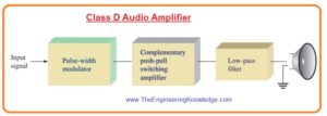
- In the below figure block diagram of class D amplifier operating a speaker is shown.
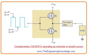
- It comprises of the pulse width modulator running complementary MOSFET output transistors working as a switch and connected with low pass filter.
- Mostly class amplifiers function on dual polarity power supplies.
- The MOSFET is push-pull amplifiers which are functioning as switch than linear devices as in class B amplifier.
Pulse-Width Modulation (PWM)
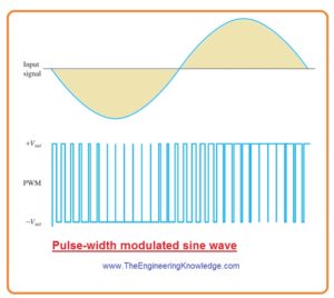
- The process in which input voltage signal is transformed into series of pulses having width which changes in proportional to the amplitude of input signal.
- This process is explained in below figure for one cycle of sine waveform.
- You can see that pulse width is wider for positive amplitude of signal and narrow for negative amplitude of signal.
- Where input is zero output is square form.
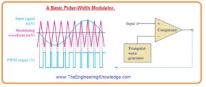
- The pulse width modulation is normally generated with the use of comparator circuitry.
- There are 2 inputs and 1 output of comparator as shown in below figure.
- The input denoted as + is known as non inverting and the input denoted as ‘-‘ is called inverting input.
- If the voltage at inverting input is larger than the voltage at non inverting input the comparator moves to its negative saturated output condition.
- If the voltage on non-inverting input is larger than the voltage at the inverting the comparator is switched to the positive output saturated condition.
- It is explained in below above figure where 1 cycle of sine waveform is given at the non inverting terminal and large frequency triangle shape wave is given to the inverting.
- The inputs of comparators are very less in range of millivolts and output of comparator is rail to rail that mean positive extreme is closer to the positive dc supply voltage and negative extreme is close to the negative dc supply voltage.
- The output of plus-minus 12 volts or twenty-four volts peak to peak is not unusual.
- From this point we can observe that gain is very large.
- For instance if input signal is ten mVpp the voltage gian will be twenty four Vpp/10mVpp=2400.
- As the amplitude of comparator output is constant for specific range of input voltage the gain is depend on the input signal voltage.
- If the value of input signal is a hundred mVpp, the output is also twenty-four Vpp and gain will be 240 instead of 2400.
Frequency Spectram
- All waves other than sine waveform are created with the harmonic frequency.
- The frequency element of specific wave is known as spectrum.
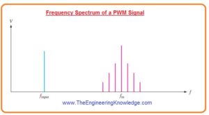
- When the triangle shape wave modulated the input sinusodial wave the resultant spectrum comprises the sine waveform frequency finput with that fundamental frequency of triangle modulating wave fm and harmonic frequency over the fundamental frequency.
- These harmonic frequencies are due to rise and fall time of pulse width modulation signal and flat regions among the signal pulses.
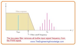
- In below figure simplified frequency spectrum of pulse width modulation signal is shown.
- The frequency of triangular waveform should be larger than the largest input signal frequency so that the less frequency harmonic is over the range of input signal frequency.
Complementary MOSFET Stage
- The MOSFETs are configured in common source complementary arrangement to give power gain.
- Every transistor changes condition among on and off state when one transistor is on other will be off. It shown in below figure.
- When transistor is operating or on then voltage about is less so very less power drop even if it has large current.
- When transistor is off current is not flowing through it and zero power dissipation.
- The power dissipation occur in transistor for less switching time.
- Power given to the load can be large since load have a voltage it almost equal to the voltage of supply and large current flow through it.
Efficiency
- When transistor Q1 is operating it deliver current to the load. Though ideally the voltage about it is 0 so internal power loss through transistor Q1 is.
PDQ = VQ1IL = (0V)IL = 0 W
- At this time transistor Q2 is not operating and current flowing though it is 0. Therefore, internal power will be.
PDQ = VQ2IL = VQ2(0A) = 0W
- In ideal the output power of the load will be 2VQIL. The max efficiency will be.ηmax
=Pout/Ptot=Pout/(Pout + PDQ)
=2VQIL/(2VQIL+0W)
= 1
- In percentage efficiency is hundred percent.
- In practical condition there some value of volts about the MOSFET in on condition.
- There is also some inner power loss in comparator and triangular wave generator.
- With that power is loss in the finite switching time therefor ideal efficiency is one hundred percent can not be obtained in practical.
Low-Pass Filter
- The function of low pass filter is that it eliminates the modulating frequency and harmonics and allow to pass original signal to the output.
- The filter has bandwidth which passes only the input signal frequency as shown in below figure.
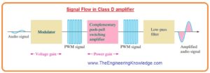
Signal flow in class D amplifier
- In below figure the signal at every point is shown of class D amplifier.
- The small acoustic signal is given and pulse width modulated to generate a Pulse width modulation at the output of modulator where voltage gain is obtained.
- The PWM operates the complementary MOSFET stage to the obtain power amplifications.
- The Pulse width modulation signal is filtered and amplified audio signal is shown on the output with enough power to operate speaker.
That is detailed post about Class D Amplifier if you have any query ask in comments. Thanks for reading. have a good day.

