 Hello fellows, I hope you all are doing great. In today’s tutorial, we will have a look at MOSFET Digital Switching. MOSFET is three-terminal semiconductor devices that have three terminals gate, drain, and source. It used in different switching and amplification applications. In the previous tutorial, we discussed the MOSFET analog switching and related parameters.
In today’s post, we will have a detailed look at the digital switching of MOSFET and related parameters. So let’s get started with MOSFET Digital Switching.
CMOS (Complementary MOS)
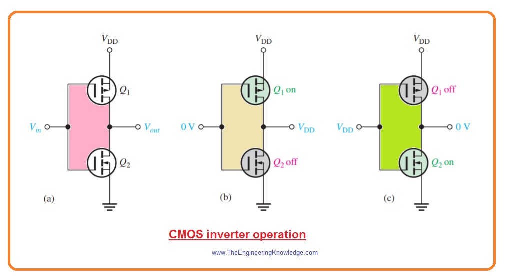
- CMOS or complementary MOS link n channel and P channel enhancement MOSFETs in a sequence as shown in the below figure denoted as ‘a’.
- The value of input voltage at the gate is either zero volts or VDD.
- Note that VDD and ground are attached to the source terminals of transistors.
- To decrease confusion the VDD is used for the positive voltage that exits at the P channel modules source terminals.
- When Vin is zero volts transistor Q1 is on and transistor Q2 is off state. It is shown in figure denoted as ‘b’.
- Since transistor Q1 is operating like closed switch the output is almost VDD.
- When Vin is equal to VDD transistor Q2 is on state and transistor Q1 is in off state as shown in figure denoted as ‘c’.
- As transistor Q2 is operating like close switch the output is attached with the ground or zero volts.
- The main benefit of Complementary MOS is that it uses very less dc power. As MOSFET are connected in series and one MOSFET remains off state so there is no current from dc source in the quiescent state.
- During switching of MOSFET there is current flow for small-time interval since both transistors are in on state for this small transition from one condition to other.
Inverter Circuit
- You can note that circuitry in the above figure can invert the input since when the input is zero volts or low the ouput is VDD or high.
- When input is equal to VDD or high the output is zero volt or low.
- Due to this reason this circuitry is known as inverter in digital electronics.
NAND Gate
- In below figure 2 extra MOSFET and 2nd input are connected with the CMOS pair to make a digital circuitry which called NAND gate.
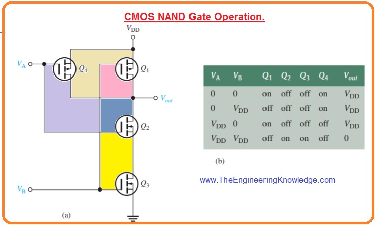
- Transistor Q4 is attached in parallel combination with the transistor Q1 and Q3 is attached in series with transistor Q2.
- When both inputs VA and VB are zero transistors Q1 and Q4 are in on state while transistor Q2 and Q3 are in off state creating Vout=VDD.
- When the value of both inputs is equal to VDD transistor Q1 and transistor Q4 are in off state while transistor Q2 and transistor Q3 are in on state, causes Vout equal to zero.
- We can observe that when inputs are not same one at VDD and other at zero than output is equal to VDD.
- This operation is practically shown in above figure table.
- It can also describe as when VA AND VB are high then output will be low otherwise output is high.
NOR Gate
- In below figure denoted as ‘a’ 2 extra MOSFET and 2nd input are connected with the CMOS pair to make a digital circuitry which called NOR gate.
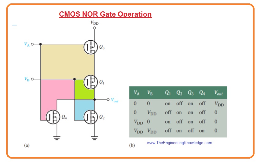
- Transistor Q4 is attached in parallel combination with the transistor Q2 and transistor Q3 is attached in series with transistor Q1.
- When both inputs VA and VB are zero transistors Q1 and Q3 are on state while transistor Q2 and transistor Q44 are in off state creating Vout=VDD.
- When both inputs are equal to the VDD transistor Q1 and transistor Q3 are in off state while transistors Q2 and Q4 are in on state causing Vout to be zero.
- We can observe that when inputs are not the same one is equal to VDD and other is zero the output is equal to zero.
- This operation is explained in the table shown in the above figure.
- It can be described as if VA OR VB OR both are high level the output is lower than output is high.
MOSFETs in Power Switching
- Before the creation of MOSFET, there was BJT power transistor. There is a need of base current to on the BJT and it has slow turn off features and is vulnerable to thermal runaway due to a negative temperature coefficient.
- While MOSFET is voltage-regulated and has positive temperature coefficient that stops thermal runaway.
- The operating speed of BJT is larger than BJT and low on state resistance causes in conduction power loss less due to BJT.
- The power MOSFET is used in motor control, dc to dc transformation, dc to ac transformation load switching and precise digital control.
Read also
- Introduction to JFET (Junction Field Effect Transistor)
- Transistor Symbols | Definition, Terminals & Operating Condition
- Difference between Vacuum Tube and Transistor
- Introduction to BC108 NPN Transistor
- What is Optocoupler,Working, Types & Applications
So that is detail post about MOSFET Digital Switching if you have any question ask in comments. Thanks for reading.