 Hello fellows, I hope you all are doing great. In today’s tutorial, we will have a look at MOSFET Analog Switching. The MOSFET stands for metal oxide field effecct transistor also called MOS transistor. It is a type of insulated gate field effect transistor which constructed with the controlled oxidation of semiconductor material. Like BJT this type of transistor has three terminals called gate, drain and source.
It used in different switching and amplification applications. In today’s post we will have a detailed look at its use as analog switching. So lets get started with MOSFET Analog Switching.
MOSFET Switching Operation
- E-MOSFET or enhancement MOSFET is used for switching applications due to their threshold characteristic VGS(th).
- If the gate-to-source voltage is less than the threshold value, there is off state of MOSFET.
- When the value of source to gate is larger than the threshold value, there is on state of MOSFET.
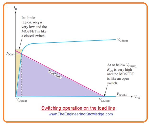
- If the value of VGS is changing among VGS(th) and VGS(on), the MOSFET is operating as switch it explained in below figure.
- In off condition for VGS<VGS(th) the transistor is functioning at the lower part of load line and behaves like an open switch or large RDS.
- If VGS is much large than the VGS(th), the component is operating at upper portion of load line in the ohmic region and behaves like a closed switch or very less value of RDS.
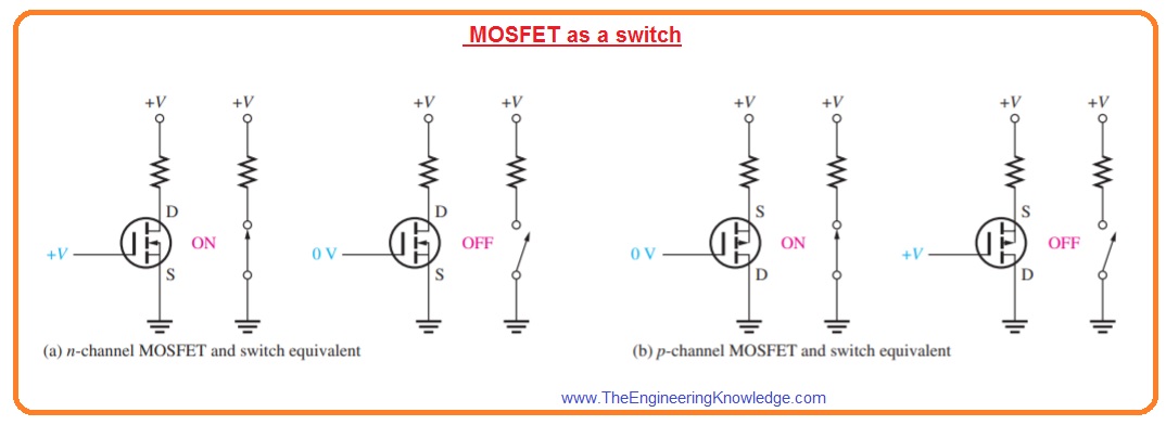
What is Ideal Switch
- In the figure denoted as ‘a’ when the gate of n channel MOSFET is +V the gate is at the more positive level than the source by quantity larger than the VGS(th).
- The MOSFET is on state and looks as close switch between the drain and source.
- If the value of gate voltage is 0 there will be zero volts for gate to source.
- The MOSFET is in off state and looks like an open switch between the drain and source.
- In the figure denoted as ‘b’ when the gate voltage of p-channel MOSFET is zero volt, the gate has a less positive value than the source by quantity larger than VGS(th).
- The MOSFET is in on state and looks like a closed switch between the drain and source.
- When the gate is +V the gate to source voltage is zero. The MOSFET is in off state and looks as an open switch between the drain and source.
MOSFET Analog Switch
- The MOSFET is usually used for switching of analog signals. Generally, a signal given to the drain can be switch through the source with the voltage on the gate.
- The main limitation is that the signal level at the source should not cause the gate to source voltage to be less than VGS(th).
- In the below figure N channel MOSFET analog switch is shown.
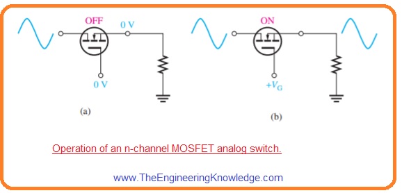
- The signal at the drain is attached to the source when the MOSFET is on through positive VGS and detached when VGS is zero.
- If the analog switch is on as shown in the below figure.
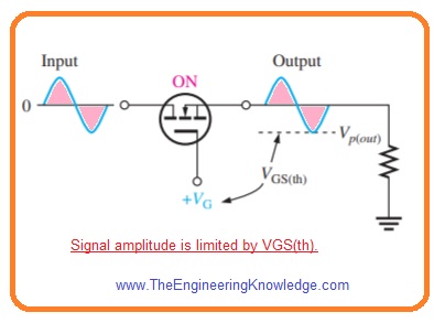
- The minimum gate-to-source voltage exits at the negative peak of the signal.
- The difference between VG and -Vp(out) is the gate to source voltage at the time of negative extreme and should be equal to or larger than the VGS(th) to retain the MOSFET in conduction.
VGS = VG – Vp(out) ≥ VGS(th)
MOSFET Analog Switch Applications
Sampling Circuit
- One application of analog switches is ADC transformation.
- The analog switch is used in the sample and hold circuit to sample the input voltage at specific ratio.
- Every sampled signal value is momentarily stored in a capacitor till it can be transformed into a digital value through ADC.
- To make this MOSFET is on for a small-time interval for one cycle of input signal through pulses given to the gate.
- In the below figure, some samples for clarity is shown.
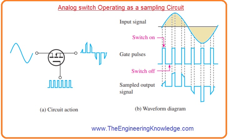
- The least rate at which a signal can be sampled and rearranged from the samples should be larger than 2 time the maximum frequency comprised in the signal.
- The least sampling frequency is named as Nyquist frequency.
fsample (min)>2fsignal (max)
- When the gate pulse has large level the switch is on and less part of the input wave existing during that pulse displays at the output.
- When the pulse wave has zero level the switch is off and the output is zero volt.
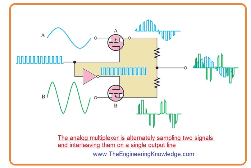
Analog Multiplexer
- For such applications where 2 signals are to be transmitted at a single point analog multiplexers are used.
- In the below figure, a 2-channel analog sampling multiplexer is shown.
- The MOSFET is on and off in an alternative fashion so ist signal sample is attached with the output and than another.
- The pulses are given to the gate of the switch denoted as ‘A’ and inverted pulses are given to the gate of switch denoted as B.
- The digital circuitry named as inverter is used for that purpose.
- For high pulses switch A is on and switch B is in off state.
- When pulses are less or low switch B is on and switch A is in off state.
- It is known as time division multiplexing since signal A displays on the output for time interval when pulse is high and signal B displays for the time intervals when the pulse is low.
- That is, they are inserted on a time interval basis to broadcast on a single line.
Switched-Capacitor Circuit
- The other applications of MOSFET in switched capacitor circuits are usually used in IC programmable analog devices which are called analog signal processors.
- As capacitors can be very easily connected in integrated circuits very easily as compared to resistances.
- Capacitors also occupy less place than the IC resistances and also lose power or no power.
- Numerous types of analog circuitry use resistances to find voltage gain and other features with the use of switching capacitors to emulate resistances dynamic programming of analog circuitry can be obtained.
- For instance, in a specific category of integrated circuit amplifiers, 2 exterior resistances are needed as shown in the below figure.
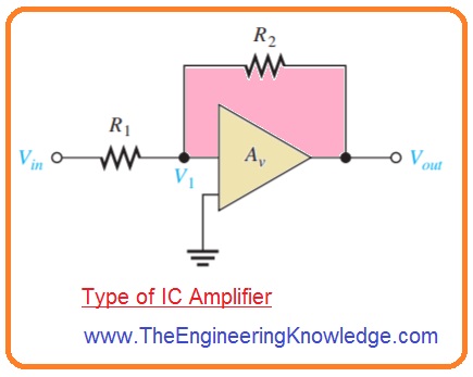
- The values of these resistances make the voltage gain of amplifier as Av=R2/R1.
- The switched capacitor can be used to emulate resistance as shown in below figure with the use of mechanical switch technique.
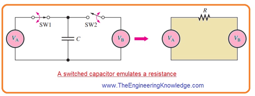
- Switch one and switch two on and off after a specific frequency for charging and discharging of C, according to values of the voltage source.
- For IC amplifiers for resistance, R1 Vin and V1 are denoted as VA and VB correspondingly.
- For resistance R2, V1, and Vout are denoted as VA and VB, respectively.
That is detailed post about MOSFET Analog Switching if you have any question ask in the comments. Stay tuned for next tutorial.