 Hello fellows, I hope you all are doing great. In today’s tutorial, we will have a look at How to Troubleshoot FET Amplifiers. The FET is a type of transistor like the BJT that uses an electrical field to regulate the movement of current. It has three terminals like the BJT first is the gate, drain and source. There is a type of FET called MOSFET, FET controls the movement of current by delivering voltage to the gate that in a result changes the conductivity between the drain and source.
There are there common types of FET amplifiers common source, common drain, and common gate. In today’s post, we will have a detailed look at the troubleshooting of the FET amplifier with the details and their related features. So let’s get started with How to Troubleshoot FET Amplifiers.
How to Troubleshoot FET Amplifiers
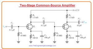
Two-Stage Common-Source Amplifier
- Let’s suppose that we have a circuit board comprising of an audio amplifier and observe that it is not functioning accurately.
- The circuit on that board is 2 stages common source JFET amplifier as shown in below figure.
- To find the issue with this circuitry we perform these steps one by one.
Step One:
- First, find the voltage level of the circuitry board so we know what to do.
- Take the datasheet of a transistor connected and find the value of gm so that we can find the value of voltage gain.
- Suppose that for specific transistors the gm is 5000 mS certain value.
- Find the resultant voltage gain for every stage according to the value of gm.
- The gm of the real components can be between certain minimum and maximum values.
- As input resistance is very large the 2nd stage does not load the ist stage circuit like BJT amplifier.
- Therefore, unloaded voltage gain for every stage is given as.
Av= gmR2 = (5000 mS)(1.5 kΩ) = 7.5
- As both stages are same so total voltage gain will be.
A’v = (7.5)(7.5) = 56.3
- Suppose that dc level is checked and verified. Now we check ac signal.
Second Step:
- Design a test setup to make the connection of input test signal, dc source, and ground to the circuitry.
- The design indicates that dc source should be plus twelve volts.
- Set ten millivolts root mean square as input testing signal.
- This value is random (though the capability of our signal source is a factor), but
less is that probable output signal voltage is less than the absolute peak-to-peak limit of twelve volts selected by the voltage source and ground - Select frequency of sine wave generator signal source to value in the audible range supposes ten kilohertz as we know that it is an audio amplifier.
- The normally audible range of frequency is from twenty hertz to twenty kilohertz.
Third Step:
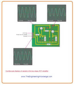
- Detect the input signal at gate of transistor Q1 and the output signal at the drain of transistor Q2 with an oscilloscope. The results is shown in below figure.
- The calculated output voltage value has peak value of two twenty six millivolts.
- The resultant peak output voltage value will be.
Vout = VinA’v = (14.14 mV)(56.3) = 796 mV peak
- The output is less from the point it should be.
Fourth Step:
- Find the signal from the output to the input to detect the error.
- The above figure shows that the oscilloscope displays the calculated signal voltage.
- The voltage at the gate of transistor Q2 is 106 millivolts peak as estimated.
- This signal is connected with the drain of transistor Q1.
- So the fault exists in the 2nd stage.
- From the oscilloscope display can be note that the gain of transistor Q2 is less than for the specific value it should be. (213 mV1/00 mV =2.13 instead of 7.5)
5th Step:
- Examine the likely reasons of the detected fault. There are 3 main reasons for low gain.
- The gm (transconductance) of transistor Q2 is less than a certain value. Read the datasheet to observe if less gm is for the lesser calculated gain.
- The value of resistance R5 is less than the value shown on the circuitry design. An errored value must display with dc voltage detection, especially if the value is different than the specific value. Therefore it is not likely to cause in this condition.
- The bypass capacitor C4 is open circuit.
- The best option to detect the gm is only to replace transistor Q2 with a new transistor of same category and recheck the output signal.
- We can make sure that resistance R5 has proper value by eliminating one end of resistance from the circuit board and finding the value of resistance with an ohmmeter.
- To stop unsolder components the best option is to separate faults by detecting the signal voltage at the source of transistor Q2.
That is a detailed post about How to Troubleshoot FET Amplifiers if you have any questions ask in comments. Thanks for reading.


