 Hello friends, I hope you all are doing great. In today’s tutorial, we will have a look at CLASS B and Class AB Push Pull Amplifier. Such amplifier which when biased at cutoff so it functions one eighty degrees in the linear region of input cycle and 180-degree cutoff this amplifier known as class B amplifier. While the amplifier operates more than one-eighty degrees of input cycle called class AB amplifier.
The main benefit of class B or class AB amplifiers over class A amplifiers is that these are much efficient than class since from these amplifiers we can get more output power from the
input. With the advantage, the disadvantage of these two amplifiers is that it is difficult to implement their circuit to get linear regeneration of the input signal. the term used for class B or class AB amplifier circuitry in which 2 transistors are operating for one half of the signal to regenerate input at the output. It today’s post we will have a detailed look at their circuit, working and related parameters. So lets get started with CLASS B and Class AB Push-Pull Amplifier. So let’s get started with CLASS B and Class AB Push-Pull Amplifier.
CLASS B and Class AB Push Pull Amplifier
Class B Operation
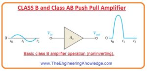
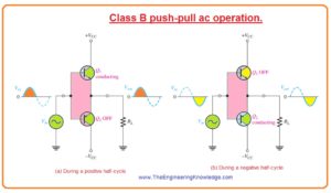
- In below figre the operation of class b is explained as the output signal is shown corosspond to input in term of time (t).
Q-Point Is at Cutoff
- The class B amplifier is bias at cutoff state so ICQ = 0 and VCEQ = VCE(cutoff).
- The class B amplifier is biased at cutoff and operating in the linear region as input signal Is operating transistor in conduction.
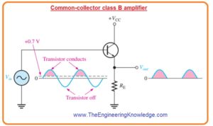
- It is explained in the below figure with a common-collector class B amplifier here output is not replicant of input.
Class B Push-Pull Operation
- In the above figure circuit shown to operate for the positive half of an input signal.
- For amplification of the complete cycle it is necessary to use 2nd class B amplifier which functions for the negative half of the signal.
- The combine operation of 2 class B amplifier is known as the push-pull amplifier.
- There are 2 main techniques for a push-pull amplifier to generate a complete signal.
- The first technique uses 2 transformer coupling while the second technique uses 2 complements symmetrical transistor which is NPN/PNP matching BJT pairs.
Transformer Coupling
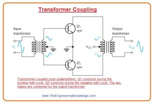
- The transformer coupling is shown in below figure.
- The secondary side of the input transformer is center-tapped which is attached with the ground generating phase inversion of one side with respect to another side.
- The transformer due to center tapping transforms input signal into 2 out of phase signal waves for transistors.
- The transformer at output link the signals by allowing the current in both directions to flow even one transistor is always at a cut off region.
- The positive power supply of the signal is linked with the center tap of the transformer connected at the output.
Complementary Symmetry Transistors
- Below shows the most used types of push-pull class b amplifier and has positive and negative power sources.
- It is a complementary amplifier since one circuitry using NPN transistor and second is using PNP which operates for both halves of the input signal.
- Note that there is no dc base bias voltage exits which mean VB is equal to zero.
- So the transistor runs in condition due to the voltage source.
- Transistor Q1 operates only a positive half cycle of an input signal and transistor Q2 operates for negative half cycle of the signal.
Crossover Distortion in signal
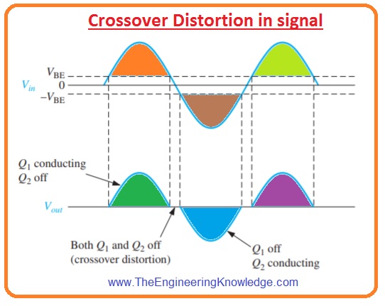
- If the value of dc biased voltage is 0 both transistors are not on and the input signal voltage should be larger than VBE before the transistor conduction.
- Due to this, there is time interval between the positive and negative variations of input when there is no transistor is operating as shown in below figure
- The resultant distortion in the output signal is known as crossover distortion.
Biasing Push-Pull Amplifier for Class AB Operation
- To reduce crossover distortion bias level is varied to reduce the voltage VBE of the transistor it causing the modification operation which known as class AB.
- In the class AB operation, the push-pull stages are get biased into less conduction mode, in a case when there is no input signal is exits.
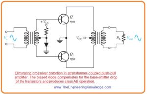
- It can be formed through the voltage divider circuit and diode combination as shown in below figure.
- The condition when the diode features of diode D1 and D2 are almost the same to the transistor base-emitter junction in this state current through diode and transistor is the same is known as the current mirror.
- This current mirror generates the required class AB operation and decreases the crossover distortion.
- In the biasing path of the circuitry shown above figure resistances R1 and R2 which has the same value like a positive and negative voltage source.
- It causes the voltage at point A among the diode to be equal to zero volts and reduces the use of the input coupling capacitor.
- The value of DC voltage at output is zero.
- By supposing that both diode and transistor are complementary are same so voltage loss of diode D1 is equal to the VBE of transistor Q1 and the voltage loss of diode D2 is equal to the voltage VBE of transistor Q2.
- As their value is the same so current of the diode will be similar to the ICQ.
- The value of diode current and ICQ can be calculated with the use of ohm law about resistance R1 and R2.
ICQ= (VCC – 0.7 V)/ R1
- This small current needed for class AB amplifier operation reduces the crossover distortion also has the potential for thermal instability if VBE of transistor loss is not the same to the diode loss or if a diode is not in thermal equilibrium with the transistor.
- Heat in power transistors reduces the base-emitter voltage and causes to increase the current.
- If diodes have a heat of similar quantity the current is in stable condition but if diode has less temperature or coll environment it causes ICQ current to increase further.
- Further heat is generated for the uncontrolled cycle which called thermal runaway.
- To continue this process there should be the same temperature condition for diodes as for the transistors.
- In some conditions, the small resistance in the emitter of every transistor can reduce thermal runaway.
- Crossover distortion also occurs in transformer-coupled amplifier which we discussed above.
- To reduce this distortion for this case 0.7 volts is given at the secondary side of the transformer which bias both transistors into conduction.
- The bias voltage to generate this loss can get from a power source with the single diode as shown in the below figure.
AC Operation
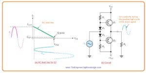
- Take the ac load line for transistor Q1 of class AB amplifier shown in below figure
- The Q point is a little bit over the cutoff point.
- The ac cutoff voltage for 2 supply functions at VCC with an ICQ is given above.
- The ac saturation for a 2 supply function with push-pull amplifier is given below.
Ic(sat)= VCC/ RL—–(A)
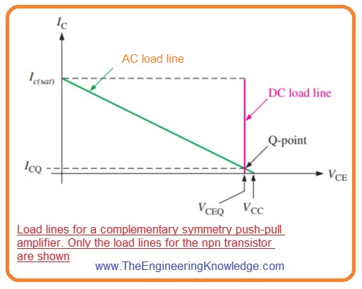
- In below figure ac load lien for NPN transistor is shown.
- The dc load line can be found by making line that passes from the VCEQ and dc saturation current IC(sat).
- Though saturation current for dc is current if the collector to emitter is short-circuited with both transistors.
- This supposed short circuit about the power noticeably would cause extreme current from the sources and infers the dc load line passes at 90 degrees over the cutoff as shown.
- The function along the dc load line that is caused by thermal runaway can generate a large current which can damage the transistor.
- The figure denoted as (a) defines the ac load line for transistor Q1 of class AB amplifier as shown in figure denoted as (b).
- In this explained condition a signal is given which swings above the region of ac load line shown in bold.
- At the upper point of the ac load line the voltage about the transistor is less and the output voltage is extreme or maximum.
- In the presence of extreme conditions transistors, Q1 and Q2 operate near cutoff to neat saturation.
- During the positive variation of input signal, transistor Q1 is operating from Q point value which zeroes to almost VCC generating a positive peak voltage a less than VCC.
- Similarly, a negative variation of the input voltage emitter of transistor Q2 is operating from Q point to zero volts to value-generating negative peak voltage almost equal to the -VCC.
- Though it is possible to function near to saturation current this type of function causes an increment in a distortion of the signal.
- The ac saturation current shown in equation ‘A’ is also the peak current of output.
- Every transistor can function over its complete load line.
- As we discussed in class A amplifier that transistors can function at complete load line with some difference.
- In class A Q point exits near the center point, there is sufficient current in the transistor with no signal.
- In class b when the signal does not exist there is very less current flows through the transistor and so there is less power dissipation.
- So the efficiency of class B amplifier can be larger than the class.
- The efficiency of class B amplifier is almost 79 percent.
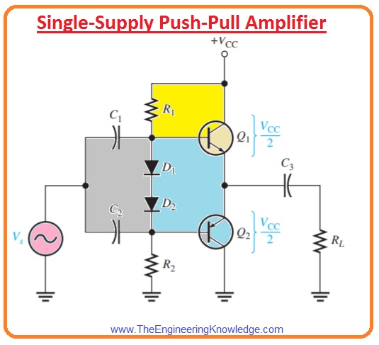
Single-Supply Push-Pull Amplifier
- Push-pull amplifier using a symmetry transistor can be functioned from the single power supply as shown in the below figure.
- The operation of the circuit is like as we discussed above with the difference is that bias is set to make output voltage at the emitter equal to VCC/2 instead of 0 volts using two power supplies.
- Since the bias is not biased at 0 volts.
- The coupling of the capacitor is necessary to stop the bias voltage from the source and load resistance.
- In ideal the output voltage varies from 0 to VCC but in practice, it does not fully fill ideal conditions.
Class B/AB Power
Maximum Output Power
- As we have discussed the ideal extreme peak output current for both dual supply and single power supply push-pull amplifier is almost Ic(sat) and the max peak output voltage is almost VCEQ.
- The ideal max average output is given here.
Pout = Iout(rms)Vout(rms)
- As
Iout(rms) = 0.707Iout( peak) = 0.707Ic (sat)
Vout(rms) = 0.707Vout( peak) = 0.707VCEQ
Pout = 0.5Ic(sat)VCEQ
- Putting value of VCC/2 in place of VCEQ the maximum average output power will be.
Pout= 0.25Ic (sat)VCC
Class B and Class AB DC Input Power
- The input power is boated from the VCC source and is given as.
PDC = ICCVCC
- As every transistor draws current for half signal the current is half wave with an average value given as.
ICC= Ic(sat)/π
- Hence
PDC= Ic(sat)VCC/π
Class B and AB Efficiency
- The main benefit of push-pull class B amplifiers and class AB over class A is their large efficiency.
- This benefit generally dominates the trouble of biasing the class AB push-pull amplifier to eradicate crossover distortion.
- As we know efficiency is the ratio between output power ac to dc input power.
Ƞ= Pout/ PDC
- The maximum efficiency for class B amplifier can be fined as.
Pout = 0.25Ic(sat)VCC
Ƞ max= Pout/ PDC= 0.25Ic(sat)VCC/ (Ic(sat)VCC/Ƞ)
= 0.25π
Ƞ max= 0.79 or 79%
- While efficiency for class A amplifier is 25 percent.
Darlington Class AB Amplifier
- In numerous applications where the push-pull configuration has used the resistance of the load is less.
- For instance, the speaker has normally used class AB push-pull amplifier.
- As we discussed above push-pull amplifiers can show very less value resistance to input resistance to the previous amplifier that drives it.
- According to previous amplifier output resistance, the less push-pull input resistance can load it harshly and highly decrease the voltage gain.
- For instance, if every bias resistance is one-kilo ohm and if a complementary transistor in a push-pull amplifier shows an ac β of fifty and the resistance of the load is eight ohms.
- The value of input resistance will be.
Rin= βac(r’e + RL)││ R1││ R2= 50(1 Ω + 8 Ω)││1kΩ││1kΩ=236Ω
- If the collector resistance of the operating amplifier is one-kilo ohm the input resistance of the push-pull amplifier decreases the effective collector resistance of the driving amplifier to the value Rc=RC ││Rin= 1.0 kΩ││236Ω = 190Ω.
- This severely decreases the voltage gain of the driving amplifier since its gain is Rc/r’e.
- In some applications, less resistance load a push-pull amplifier with Darlington transistor can be used to increase input resistance used to drive the amplifier and avoid severe decrement the voltage gain.
- The net ac β of the Darlington pair is usually denoted in excess of a thousand.
- With that bias, resistance can be large since the base current is needed.
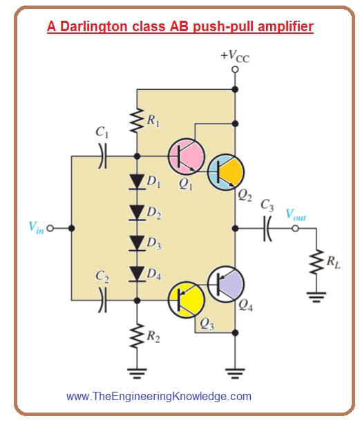
- The Darlington class AB push-pull amplifier is shown in the below figure. 7.19
- There is a need of 4 diodes in the bias circuitry to fulfill the 4 base-emitter junctions of 2 Darlington pair.
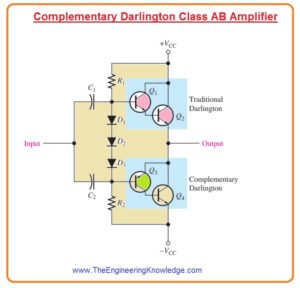
Complementary Darlington Class AB Amplifier
- The complementary Darlington also called Sziklai pair.
- It is like the Darlington pair with the difference is that it has different categories of transistors one NPN second is PNP.
- the below figure shows the class AB push-pull amplifier with 2 NPN output power transistors denoted as Q2 and Q4.
- The upper portion of the push-pull circuit is normal Darlington pair and the lower portion is complementary Darlington.
So, friends, it is a detailed post about CLASS B and Class AB Push-Pull Amplifier if you have any queries ask in the comments. See you in the next tutorial. I tried my level best to make it simple for you.
Read also:
- LM324 – Single Supply Quad Operational Amplifiers worksheet
- Difference Between An Operational Amplifier and Comparator
- Amplifier circuit using LA4440 IC
- Introduction to LM258 Dual Operational Amplifier IC
- Introduction to 2sc828 NPN Amplifier Transistor
Faqs
- Class AB amplifiers join the strengths of Class A and Class B amplifiers. The class ab amplifiers come with good signal regeneration of class A amplifiers and a complementary pair of transistors of class B amplifiers that has good efficiency.
- Class B amplifiers are effective with low fidelity but generate high distortion. These amplifiers provide high fidelity and efficiency. The push-pull pair of output transistors in the Class AB amp is one more thatn half of the time and not On and OFF suddenly.
- Two class B amplifiers configured like one amplifies positive half cycle and the other amplifies negative half cycle are called push-pull Class B amplifiers.
- Push all Class B amplifiers can made with the use of two same-type transistors or two complementary transistors.
- The cross-over distortion in the class B power amplifier is reduced with the class AB power amplifier that uses diodes at the base of a transistor for reducing forward biased voltage at the base through biasing the transistor above the cut-off.
- Class d is common to use, it is only used at the starting time for bass because of high amount of noise produced
- If class B amplifiers amplify the signal with two active devices that operate on one-half of the cycle. Efficiency is well for class A amplifiers. Class B amplifiers are best for battery-operated devices like transistor radios. Class B comes with maximum theoretical efficiency of π/4 (≈ 78.5%).




This is a site that inspires me and informs me correctly, which is why I
want to tell you how I managed to overcome the loss of
my work from home, I hope it will help other.
Fantastic article…thanks for sharing such an amaing content with us.Good job.Keep it up.