 Hello, friends, I hope all of you are enjoying your life. In today’s tutorial, I am going to explain Difference Between Single Sided PCB & Multilayer PCB. PCB stands for printed circuit board also known as printed wiring board. When it was not common to use circuit construction was a very difficult and time-consuming process also costly, because it was done manually. Manually constructed circuits also had less working life and insulation of these circuits was difficult. After the availability of integrated circuits and different semiconductor materials circuit compositions became easy and the printed circuit board also developed with time.
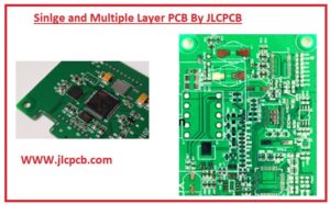
This circuit board made the construction of circuits too easy, cost-effective, and increased reliability. Now on this board, we can easily make our circuits and projects. With provide you with a detailed overview of single and multilayer also want to give a detailed overview of the PCB manufacturers that can help you to make PCBs for your projects with high quality and affordable prices. There are numerous PCB suppliers are working but only the best PCB manufacturer is JLCPCB. Over 800,000 businesses and innovators use JLCPCB. Whether you’re creating your first PCB, or developing an electronic hardware product, they are here to help you build hardware easier and faster by providing rapid PCB prototype and SMT assembly service. JLCPCB constantly looking for new ways to improve and shorten the PCB prototyping process — from pioneering online quoting/ordering system, and automatic production to fast delivery. JLCPCB makes the cheapest but top-quality PCBs possibly because of scale effect, extremely high production efficiency, and less manpower cost.

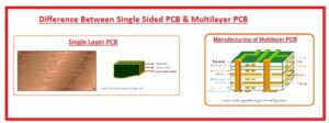
Single-Sided PCB Board
- Single side PCB baord comes with a single layer of conducting material on one side and its other side has electronic component connections.
- These boards are made with substrate layers, conductive metallic layers, and solder mask applied and silkscreen exists on board.
- First-time the single board was made in the 1950s and used as the first technology for PCB board. Still, it is used in different projects and circuits.
Features of Single-Sided PCB
- These boards are low cost and come with high volume orders.
- It is best to use for low-density designs and can manufacture easily.
- Its designing process is easy and preparing is also a simple process
Construction of Single-Sided PCB Board
- The single-layer board comes with conductive layers and has base materials that provide structural support to the board.
- Substrate materials used for the creation of these baord define where it has to be used and how much it is rigid and flexible.
- The thickness of foil over the conductive layers can be different according to applications that are defined in ounces per square foot.
- A solder mask is applied over the copper traces to avoid corrosion, short circuits, and other environmental factors.
- At last silkscreen layers are applied that show different symbols, numbers, values, and details for components connections and circuits.
Vias in multilayer PCB
The types of vias are used in this board
- Through-hole Via
- Blind Via
- Buried Via
Through-hole Via
- This type of via passes through complete layers of boards to connect them. It has a larger diameter as compared to vias and with the use of the drilling process it made
Blind Via
- This via made through the external layer of the board to the inner layers not making holes passing in the board. These vias are also called blind vias since not have holes on the other side of the board. These holes are made with certain dimensions according to board measurements. The main use of these vias is to connect the external and internal layers of the board.
Buried Via
- This visa is used for making the connections between 2 or more inner layers of the board and not passing through inner layers. In multilayer boards inner plating of buried vias should completed before using 2 external layers of board. Buried vias are high cost since they provide high accuracy for design.
Multilayer PCB
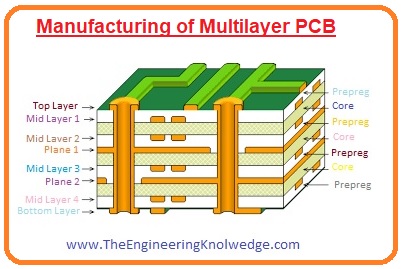
- The multilayer PCB board comes with 3 or more conductive copper layers. The double-sided board has two conductive layers on the upper and lower of the PCB substrate.
- This board’s inner layers core are in central layers and coated with copper layers on two sides and prepreg works as an insulator.
- Two external layers are single-sided boards and the inner layers are double-sided.
- In this board, all layers are configured with each other through copper-plated holes and normally it has 40 layers.
- Different components used for component creation such as active and passive are connected on upper and lower layers and the inner layers mainly work as routing.
- Four to eight layers are used in smart devices and mobile phones 12 layers are used.
Single layer PCBs vs. Multilayer PCBs
- The single-sided board is the basic type of PCB board that has components on a single side. It comes with conductive layers and also substrate layer.
- In the case of multilayer boards, we can connect components on two sides, and comes with more than 3 layers based on features. The multilayers are stacked with each other. In this board core is between prepreg layers and copper-coated layers. Multilayer boards have an even number of layers.
- Single layers board is low cost and designing is an easy process and made without any complicated tool use.
- The design of a multilayer board is complicated but they are durable as compared to a single-layer board. They have features to handle high-temperature conditions and other features
- The repairing process of multilayer boards is difficult and needs advanced machines and skills. While single-layer boards can easily repaired.
- The use of multilayer boards is in aviation, medical devices, and aerospace. Single layers board used for calculator, coffee machines solid state driver, etc Read our More Engineering Blogs
| Feature | Single-Layer PCB | Multilayer PCB |
| Layer | one conductive layer. | Two or more layers |
| Complexity | less complex | It is highly complicated since has larger layers |
| Design Flexibility | limited design. | High design flexibility |
| Cost | low cost | High cost |
| Production Complexity | simple and easy. | complicated |
| Component Density | Low component density | High component density i |
| Signal Integrity | Low due to limited shielding | Good signal quality |
| Applications | Simple functions in devices | Used for high-performance electronics, advanced functionality, and miniaturization. |
| Size and Weight | Larger | Small size and low weight |
| Use | Toys, | telecommunications system, computer |


