Hello, readers welcome to the new post. In this post will learn the Construction of Single Layer PCB. PCB full forms printed circuit also called a printed wiring board. Before the use of PCB for the circuit creation process was very difficult and expensive since manual methods were used to create circuits. Then with the use of PCBs, the circuit creation process becomes very easy and less expensive.
According to different features and applications different types of PCB were designed and used in different projects. Each category of PCB has its use and applications. From basic to complicated devices are created through the use of PCBs. In this post, we will learn about the single-layer PCB its construction, applications, and some related parameters.
What is Single Layer PCB
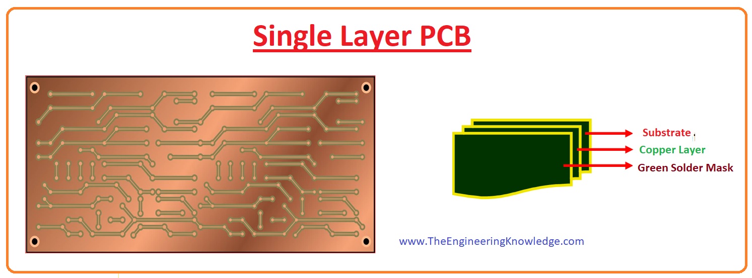
- Single-layer PCB is also named as single-sided PCB this category of PCB has a single layer where a conductive path occurs.
- Its one side is used for the creation of projects and circuits their side is not used for project creation.

- This category of PCB is generally used at different projects and devices due to its low cost and easy manufacturing.
- Different material is used for the creation of single-layer PCB like phenolic resin with a combination of copper foil and glass fiber.
- It is called a single-layer PCB since it consists of a single conductive layer. Compact circuit preferred this board.
- Over the other types of PCB single layer, PCB is very commonly used in different applications.
- In the case of complicated projects, another category of PCB is preferred but for basic projects, single layers is used.

Types of Single Layer PCB
- Different types of single-layer PCB are described here with the detail.
Single Layer Flexible PCB
- It is created with the use of flexible substances like plastic. Its manufacturing process is expensive.
Single Layer Rigid-Flex PCB
- The circuits designed with this PCB is used for such projects where the high frequency is used.
- It is constructed with Teflon. To use it practically some parameters are considered such as absorption of moisture, dielectric loss, thermal expansion
Single Layer Aluminum PCB
- In this PCB the substrates material is created with the use of aluminum.
- Its structure is like the copper substrates but the difference having aluminum as a substrate.
Single Layer Rigid PCB
- In this kind of PCB, there is the use of rigid substances for the creation of board such as fiberglass.
- Due to inflexing nature helps to save the circuitry from damage and breaking.
- Its common applications are power supply and electronic devices.
Cost of Single Sided PCB
- after getting the detailed overview of the single-sided PCB now discuss the price details through which you can buy this board.
- Due to one conductive layer and easy design and simple layout, its construction is done at less price.
- Different PCB manufacturers offer the single-layer boards in different prices but JLCPCB is the most reliable and famous PCB designer that can help you to make PCB at a very less cost and with high quality and reliability features.
- It Founded in 2006, JLCPCB has been at the forefront of the PCB industry. With over 15 years of continuous innovation and improvement based on customers’ needs, they have been growing fast and becoming a leading global PCB manufacturer, which provides the rapid production of high-reliability and cost-effective PCBs and creates the best customer experience in the industry.
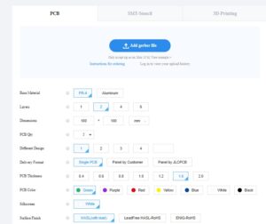
- To place an order move to the JLCPCB website and press on the button order now after that new interface shown below can be seen

- In the above figure, we can see that different options related to layers are shown like 1, 2, 4, and 6. You can select according to your requirements but for a single layer press at 1.
- With that there are different options are also shown like base material, dimensions, etc that you can select according to you’re requirements.
- By selecting the single-layer order you can get the five pieces in just two dollars
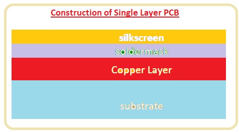
Construction of Single Layer PCB
- The construction process of single-layer PCB is described here with the details.
Board Cutting
- Here base material is chosen on the basis of data sent by the customer. Normally FR-4 is used bt in some applications there is used of aluminum coppe.
- After that cleaning and cutting of board is done that can be handled by machine dimensions.
Drilling
- To position, the different circuit elements and heat sinks drilling is done and also for lead elements.
- The drilling process also helps to link the different layers. For multiple layers, connection vias are used.
Electroplating
- After drilling there is a coating of chemicals is done on the board. Copper is positioned in the vias of the board to make the links among the layers.
Plating with Copper
- In copper, plating is applied and the quantity of applied copper depends on the user’s needs.
Printing of CIrcuiry
- To draw the design and different circuits layers on the board there is photo resistive material is used. For this process, such a place is used where white light does not exist.
Removal of Undesired Copper
- In this step, there is the elimination of non-desired copper relies on the board. This process is called etching.
- The different solutions are used to eliminate the copper such as copper chloride, hydrogen chloride.
Automatic Optical Inspection
- To detect the different faults existing in the board AOI inspection is done on the board. Different cameras at positioned at certain angles are used.
Application of Solder Mask
- A polymer layer is applied on the board called a solder mask and it comes with different colors combinations.
- It helps to avoid the solder bridges on the board.
Flying Probe Testing of Board
- Final testing is done on the board voltage is given through probes to detect the open circuit and short circuit points on the board.
- After complete inspection board is moved through packaging and customer delivery
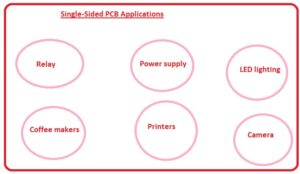
Single-Sided PCB Applications
- The common applications of single-layer PCB are described here.
- It is used in timers circuits.
- It used in the circuit creation of radio
- It employed in relay circuits
- It is a circuit of power supply.
- It used in sensor projects
- LED lights consist of single-layer board
- Solid-state drivers used this board
- Vending machine used this board

Advantages of Single-Sided Board
- Different advantages of the single-sided board are explained here
- Its layout is very simple since consists of one layer of conductive material and can be easy to design
- Due to being simple and easy to construct is available very easily for projects
- Its price is very less
- Simple design makes it reliable for different projects
- Its testing and Maintainance in case of fault is simple and less costly
Disadvantages of Single Layer PCB
- With the benefits of this board, it has some drawbacks that are listed here.
- Its area is larger than other boards and makes it less effective for different applications
- It is not preferred for complicated circuits
That is all about the Construction of Single Layer PCB. I have explained all details about the Construction of Single Layer PCB. If you have any further query ask in the comments. Thanks for reading have a good day


