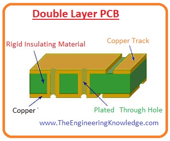
Hello, readers welcome to the new post. In this tutorial, we will discuss Construction of Double Sided PCB. The double-sided board is made with two copper layers at the upper and lower sides. The copper pads and copper traces exist on board sides and two copper layers are configured with plated through holes. These boards do not have inner layers
This type of board is a low-cost option for different electronic projects and devices. For double side boards components are connected on both sides.
. The most reliable and high-quality PCB supplier is PCBWAY which can offer PCB-related services they offer single as well, as double-sided PCB boards with high-quality and affordable features and requirements.
PCBWAY is located in China creating more than twenty-one hundred PCB board pieces per day. They come with features of PCB prototyping, assembly designing with CNC, and three-D printing features in a single place. By investing in new tools, quality control, and user support, PCBWay provides quality services at very competitive prices. The company stands out for its support for a wide range of technology and an easy-to-use website, but above all for its strong community support
Another popular tool on the PCBWay site is a list of the most common PCBs, price by volume measurements, and other parameters found in the easy-to-read chart. This allows consumers, for example, to freely estimate how much it will cost to order 100-layer PCBs or 500 aluminum boards. Each service has its place on an accurate website but can still be easily accessed from the main web page. Once you have used the service of your choice, a quick quote can give you an estimate of the cost of your project and direct you to the official order form used to request a formal, detailed quotation.
Another popular tool on the PCBWay site is a list of the most common PCBs, price by volume measurements, and other parameters found in the easy-to-read chart. This allows consumers, for example, to freely estimate how much it will cost to order 100-layer PCBs or 500 aluminum boards. Each service has its place on an accurate website but can still be easily accessed from the main web page. Once you have used the service of your choice, a quick quote can give you an estimate of the cost of your project and direct you to the official order form used to request a formal, detailed quotation.

Double Sided PCB Stack-up
- The upper layers of double-sided boards come with conductive layers. then the dielectric layer is applied which is called the base material. At the lower part of the board, there are other conductive layers. Dielectric layers are between two conductive layers.
- The conductive layer is made with copper and comes with good electrical conductivity features and a low-cost board. Gold or silver is used for making conductive layers.
- the base layers are made with the use of different materials such as FR4, polyimide, PTFE, and metals and are configured on the substrate.
- Sometimes non-conductive base materials are used that work as insulators for two upper and lower conductive layers.
- If there are base layers made with metal then dielectric layers are used for insulation between layers to control short circuit
- Over the base and conductive layers there is surface finishing, solder mask and at last silkscreen layer applied.
- Surface finish used for protection of copper layers and avoid oxidation and corrosion on board.
- Solder mask used for stopping the creation of solder bridges and undesired connections. The silkscreen has labeling details of the components connected.
Types of double-sided printed circuit boards
Rigid Double-sided PCB:
- It is the basic type of double-sided board made with the use of FR4 materials and is best ot used for handling electrical features and low cost option
Flexible Double-sided PCB:
- It is made with use of polyimide materials and comes with a good flexible nature and low-cost features. It is used for projects that need low-weight
Flex-Rigid Double Sided PCB:
- It comes with a rigid and flexible material and has features of both flexibility and rigidity.
Metal Core Double-Sided PCB:
- This board comes with copper, aluminum, and some other metals. So best for heat dissipation and used in LEDs devices
DFM Check:
- DFM is a process used for board manufacturing and this process helps to check copper, solder mask, silkscreen, and drilling through using software and offers details for board manufacturing. If there is any issue found in the DFM report ask customers to provide the required details and solve the issue for proper manufacturing
Penalization Process :
- The penalization helps to provide details for ups set on the standard panel used for production. Then get different penalization results such as core scaling, maskless results, draw results, drill output, and etching testing. That rough data is forwarded to make a board.
Panel Cutting:
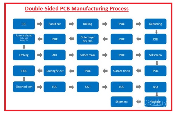
- In this step material reached at manufacturing point in the form of a larger sheet of about 41*49’’. There is a need to cut board materials based on board thickness features.
Drilling:
- Here boards are configured with fixtures to get the required drilling process. then drilling program was added to the drilling machine and the drilling machine made holes based on board drill layers. In some applications via fill, blind vias, and buried vias are used for that applications special processes are used.
Copper Plating:
- In this step, copper plating is applied on the PCB surface making boards thick and offering copper connection with layers of surface pads. The boards are drilled for connection layers with layers.
Imaging Outer Layers:
- this method is used for transferring circuits on copper through the use of films. The image transfer there is a need for protection film. With that oxidation not used for the surface so clean board.
Inspection of Outer Layers:
- Check the image’s accurate registration of external layers. Normally this phase checks short circuits, broken connections, and if there is alignment of the board. AOI is used for checking these errors and providing results in image form.
Etching:
- This phase needed to remove undesired copper from the board. When etching is complete, circuit images exist on board. Etching is done with the use of chemical solutions.
Applications of Mask:
- Solder mask is used on copper layers.
Silkscreen Printing:
- Silkscreen is applied on the board that has details of components connected, different parts, symbols, etc
Surface Finish:
- In this process, surface finish is completed by using different methods of PCB surface finishings.
Single-Sided vs. Double-Sided PCBs
Single-Sided PCB
- It comes with single conductive layers
- Components are connected on one side
- it has routing on a single side.
- It has low component density.
- its signal quality is poorer than double-sided
- It is large size board and is used for simple circuits
- Low-cost board
Double-Sided PCB
- It has two conductive layers
- It has component connections on two sides
- It is flexible and has high space for component routing
- Its component density is higher
- It has a ground plane on a single side.
- It is a compact design board used for high-frequency applications
- it is a costly board
Read also:
- How to Manufactured Large PCB Board
- Main Parts of PCB Board
- Difference between Double sided and Multilayer PCB Board
- Build Your Own PCB Board


