 Hello friends, I hope you all are doing great. In today’s tutorial, we will have a look at Introduction to Step Tunnel Diode. The tunnel diode is also known as Esaki diode is a type of diode that has a large value of negative resistance. During working at Tokyo Tsushin Kogyo in 1957 Esaki, Yuriko Kurose and Suzuki first time created the tunnel diode. Due to the creation of the tunneling effect used in tunnel diodes Esaki got the Nobel Prize in Physics.
The PN junction of tunnel diode is highly doped from positive to negative almost ten nanometers. Normally these diodes are constructed with the germanium can also be created with the gallium arsenide and silicon. In today’s post, we will have a detailed look at its working, construction, features and some other related parameter. So let’s get started with Introduction to Tunnel Diode.
Introduction to Tunnel Diode
- The tunnel diode has a high level of doped PN junction and its current reduces with the increment in voltage.
- There is some special feature of this diode that makes it distinctive than other diodes is negative resistance.
- Due to negative resistance mostly used in oscillator and microwave amplifier circuitry.
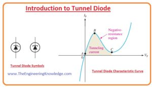
- The symbols of tunnel diode are shown in the below figure.
- The doping level of tunnel diode is larger than the normal diode used in rectifier circuits.
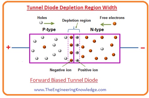
- Due to the high level of doping decreases the area of the depletion region.
- Due to the thin depletion region the current can flows through the diode in reverse biased condition, there are no breakdown effects exits for this diode similar to a normal diode. It is shown in the below figure.
- Due to less depletion region electrons crosses the pn junction at very less value of forward biased voltage and current flows through diode.
- In the figure, you can observe these phenomena at points A and B. with the further increment in forward biased voltage-current start to decreases after point B. This part of the curve is known as a negative resistance region.
RF = ΔVF/ΔIF
- The factor of a diode is opposite to Ohm’s law that say with the increment of voltage-current also increases. At point C of the curve, the diode starts operating like the normal diode.
Tunnel Diode Depletion Region Width
- The depletion region of any diode is a part of a diode where positive and negative ions are existing.
- It is a barrier that stops the flow of electrons from the N region of a diode to P region and holes from the P to N region.
- The area of the depletion region relies on the concentration of the impurity added in the diode.
- Impurities are added in the N and P parts of a diode to enhance their electrical conductivity.
- If the impurity adds in less concentrations the area of depletion region is less and if the concentration of impurities is large than the area of the depletion region is large.
- In tunnel diode, the doping level is high means a large concentration of impurities added in a diode.
- Due to high doping, the area of depletion region is less. The impurities added in tunnel diode has concentration almost one thousand times larger than a normal diode.
- The depletion region of the conventional diode is larger than the tunnel diode. This large area reduces the flow of current.
- Due to the large area depletion region function as a barrier. To cross this barrier there is a need for some amount of voltage.
- When a certain value of voltage provided to diode current starts to flow through the diode.
- While the depletion region of tunnel diode is less as compared to normal diode so the less amount of current will generates a current in tunnel diode.
- The stability of tunnel diode is longer than normal diode so it mostly used in high-speed operation circuits.
Tunneling in Tunnel Diode
- The depletion region of diode consists of positive and negative ions that are connected through the electrical field.
- The for exerted by the field of the depletion region is opposites to the applied by the exterior voltage source.
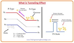
- As we know that the valance and conduction band in N-type semiconductor substance is less than the valence band and conduction band of P-type material.
- The alteration in energy value is due to variation in doping level in N and P materials.
Tunnel Diode Construction
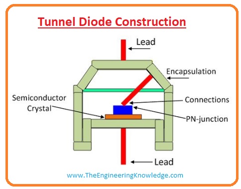
- There are 2 terminals of diode first is positive called anode and second is negative called cathode.
- The P portion of the diode operates as anode and the N part is denoted as a cathode.
- The material used for a tunnel diode is germanium and gallium arsenide.
- The doping level of tunnel diode is a thousand times larger than the normal diode.
What is Tunneling Effect
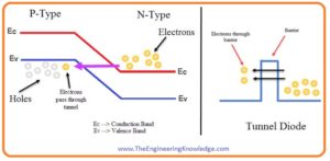
- The flow of electrons from the N side to P side after crossing the potential barrier or depletion region is known as tunneling.
- In the conventional diode depletion region is a combination of positive and negative ions.
- These ions field applied force opposites to the exterior applied force.
- With the decrement in the depletion region of diode, charges can move across the potential barrier, for this crossing, there is no need of any kind of energy for charges.
- This process is known as tunneling and due to that fact diode called tunnel diode.
- The tunneling effect generates a high value of current for the less value of forward biased voltage.
- So diode can function in both forward and reverse biased conditions.
- The decrement in area of depletion region also reduces the reverse breakdown voltage.
- This less reverse voltage causes the breakdown of a diode. Henceforth, this makes a negative resistance region.
Tunnel Diode Working
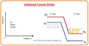
Unbiased Tunnel Diode
- When there is no external supply is provided to diode then a highly doped conduction band of N part of diode will merge with the valence band P part of diode.
- At this condition, the electrons existing in N region will mix with the holes of the P region and they have same energy level.
- With the increment in temperature the electrons exiting in the conduction band of N partition move to the valence band of P portion.
- The holes of P part will move to N condition band in N portion.
- Due to equal holes and electrons movement, there will be no current flows in the diode.
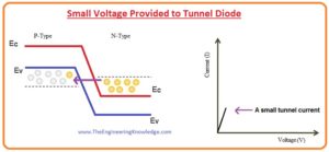
Small Voltage Provided to Tunnel Diode
- If we apply less value of the voltage to diode the small number of electrons flows across the barrier from N region to P region.
- Due to small voltage-current start to flow in less quantity.
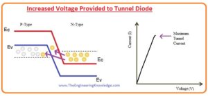
Increased Voltage Provided to Tunnel Diode
- If we increase the voltage provided to diode the generation of electrons and holes in N and P region also increases.
- Voltage increment increases the combination of bands of a diode.
- The current flowing increases with the N region valence aband and P region conduction band has the same energy level.
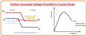
Further Increased Voltage Provided to Tunnel Diode
- If we further increase voltage provided there will be variation in their alignment of conduction and valence band.
- But at this point still, some overlapping between conduction and valence band of N and P region.
- The current also flowing from N to P region but with voltage increment, its quantity decreases.
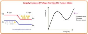
Largely Increased Voltage Provided to Tunnel Diode
- If we increase the applied voltage to an extreme point there will be a decrement in current flowing through the diode.
- The conduction and valence band will not be overlapped at this point and electrons movement is zero and tunnel diode is operating like the normal diode.
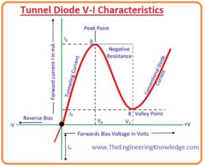
Tunnel Diode V-I Characteristics
- For forward biasing conditions current start to flows through the diode due to a large doping level.
- In given below figure characteristic curve of tunnel diode is drawn between Ip and Vp.
- The current across the diode will be the highest IP when the voltage across the diode is Vp.
- If we increase the voltage across the diode further than the current flowing diode will decrease.
- This least value of current flowing through a diode is known as valley current Iv.
- In the figure, you can see that from point A to point B current reduces with the increment in voltage.
- Thus from A to B the resistance offered by the diode is negative resistance.
- In this part of curve diode generating power instead of using.
Negative Resistance in Tunnel Diode
- In the above curve, you can observe that with the increment in voltage provided current start to reduces from point Iv to Ip.
- The part of the curve is called a negative resistance region.
- In this part of the curve, the diode generates power instead of using it.
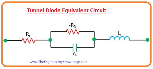
- In the below figure equivalent circuitry of the tunnel diode is shown.
- The Rs is the resistance offered by the connection between diode and semiconductor material.
- The value of this resistance is five ohms.
Tunnel Diode Applications
- These are some applications of the tunnel diode.
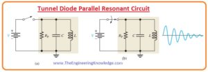
Tunnel Diode Parallel Resonant Circuit
- The parallel resonant circuitry can be constructed by using capacitor, inductor, and resistor in parallel combination. In denoted in a circuit (a).
- The resistance Rp connected in parallel is the resultant of the series winding resistance of the coil.
- When the input voltage is provided to circuitry than the damped oscillation is generated.
- The damped oscillation is produced due to the resistance offered by the tank that stops the continued oscillation since power is lost when current flows through a resistor.
Tunnel Diode Oscillator
- If we add tunnel diode in series with the tank circuitry and provide voltage to diode at the center portion of the negative resistance part of the characteristic curve.
- The output voltage for this case will be a constant sine waveform.
- It is due to the negative resistance characteristics of the tunnel diode will counter the positive resistance offered by the tank circuitry or resonance circuit.
Tunnel Diode Advantages
- These are advantages of tunnel diode.
- Its operating life is longer.
- Its operating speed is high.
- It creates less noise during operation.
- It uses less power.
Tunnel Diode Disadvantage
- These are some disadvantages of tunnel diode.
- Its input and output terminals are not separated from each other.
- These diodes are constructed in limited numbers.
Related Posts
- Current Regulator Diode
- Zener Diode
- Step Recovery Diode
- PIN Diode
- Schottky Diode
- Photodiode
- Varactor Diode
- Diode
- Zener diode Applications
- Laser Diode
- LED
So friends that complete post about a tunnel diode I have mentioned each and every parameter related to tunnel diode. If you have any further queries about this diode ask in comments. See you in next post have a good day.


You really make it seem so easy with your presentation but I find this matter to be really something which I think I would never understand. It seems too complex and very broad for me. I’m looking forward for your next post, I’ll try to get the hang of it!