 Hello friends, I hope you all are doing great. In today’s tutorial, we will have a look at Introduction to JFET (Junction Field Effect Transistor).The full form of JFET is a junction field-effect transistor. The normal transistor such as BJT is used to control current or we can say current controlling device. While the JFET is a voltage control component. As we know normal transistor has three components which are emitter, base, and collector.
Similarly, there are three main terminals of JFET which are Gain, Drain, and source. There are 2 main types of FET transistors in which JFET is and the second is MOSFET. In today’s post, we will have a detailed look at its structure, working, features, and applications with the detailed. So let’s get started with an Introduction to JFET (Junction Field Effect Transistor).
Introduction to JFET (Junction Field Effect Transistor)
- The JFET is a type of field-effect transistor that is used in amplifier circuits, voltage-controlled resistance, and as a switch.
- As bjt control current JFET is used to control the voltage.
- In JFET there are two types of channels first one is n-type and the second one is a P-type channel.
- For the reduction of current in N-type JFET, the voltage given to the gate should be negative concerning the source.
- Similarly in P-type the voltage given to the gate is positive concerning the source to decrement in the current.
- The JFET input impedance is higher and usually has a value of 1010 ohms, it means there is no effect on the exterior component linked with its gate.
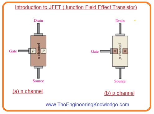
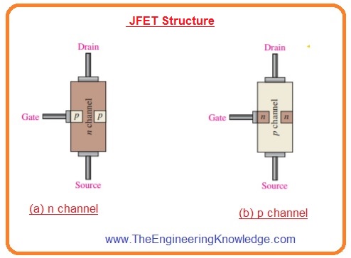
JFET Structure
- The figure denoted as ‘a’ shows the structure of the n-channel junction field-effect transistor.
- The wire is attached to every endpoint of N channel the drain is at the top point and the source is at a lower point.
- In n channel configuration, 2 p-type materials are diffused with the n-type material to construct a n-channel and both p-type regions are attached with the gate terminal.
- To make a simple configuration gate is linked with only one p region.
- In figure a the configuration of P channel is shown which is similar to the N channel with a difference of diffusion of materials.
Working of JFET
- To discuss the woking of junction field-effect transistor below figure shows dc bias voltage given to the n channel of JFET.
- VDD is delivering the drain to source voltage and current is flowing from drain to source.
- The VGG giving thee reverse bias voltage among the gate and source as shown in below figure.
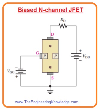
- The junction field transistor operates with the gate-source pn junction in reverse bias condition.
- Reverse biasing of gate-source junction with the negative voltage generates a depletion region in the PN junction that increases the area to the n channel and so increases resistance by limiting the area of the channel.
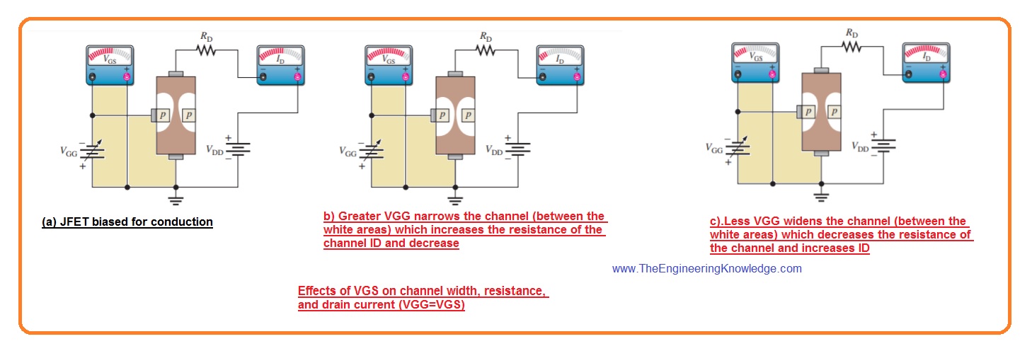
- The area of channel and channel resistance can be varied by changing the gate voltage by changing the quantity of drain current ID.
- The below figure explains this factor. The white color area denoted depletion region formed through reverse biasing.
- It has large area towards the drain end point of the channel since the reverse biased voltage among gate and drain larger than the voltage among the gate and source.
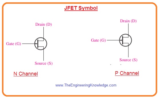
JFET Symbol
- The symbolic representation for both N and P channels is shown in the below figure.
- You can see that there is in arrow for a gate in n channel and out for the p channel.
JFET Drain Characteristic Curve
- Suppose that the gate to drain voltage value is 0 or VGS=0. It is generated by linking the gate with the source as shown in the figure denoted as ‘a’. Here both source and gate are connected with the ground.
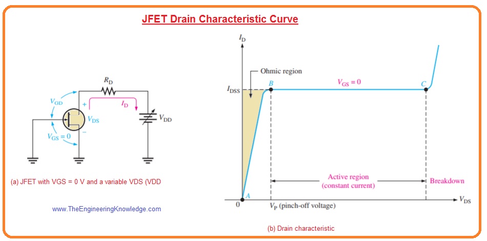
- With the increment in VDD from zero volts ID will rises in direct relation as shown in graph in the figure among points A and B.
- In this region, the resistance of the channel is constant since the depletion region is nor large to have any effect.
- It is known as ohmic region since VDS and ID are relating to each other through ohm’s law.
- At point B of a graph, the curve levels off and goes into the active region there the current ID is constant.
- With the increment in VDS from point B to C, the reverse bias voltage from gate to drain generates a depletion region larger such that to offset the increment in VDS by maintaining the current ID constant.
JFET Pinch-Off Voltage
- For the value of voltage VGS =0, the value of voltage VDS at which drain current ID is constant is called pinch-off voltage (VP) it denoted as ‘b’ in above graph.
- For specific junction field-effect transistors, the value of VP is constant.
- We can observe that the continuous increment in voltage VDS over the pinch-off voltage causes a constant drain current.
- This value of drain current is called IDSS or drain to source current with shorted gate and is mentioned on the datasheet of junction field-effect transistor.
- IDSS it the highest drain current in which a certain junction field-effect transistor can generate irrespective of exterior circuitry and always denoted for condition VGS is equal to zero volts.
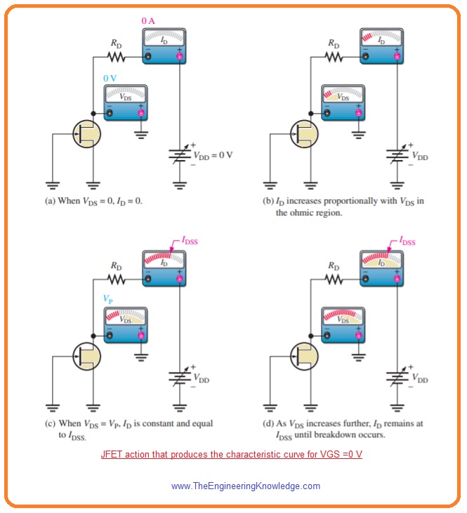
JFET Breakdown
- In the above graph, you can see that the breakdown exits at point C when the current ID starts to increase very fastly with an increment in voltage VDS.
- A breakdown can damage the transistor permanently, so it always operates less this breakdown value in the active region which is shown on the graph among points B and C.
- The junction field-effect transistor action that generates the drain characteristic curve to the value of breakdown for voltage VGS is equal to zero is explained in below figure.
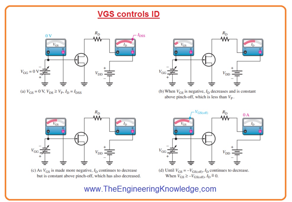
VGS Controls ID
- Let us connect a bias voltage VGG from gate to source according to a given configuration as shown in below figure denoted as ‘a’.
- As VGS is increasing toward negative value by varying VGG the group of the characteristic curve is generated as shown in the below figure denoted as ‘b’.
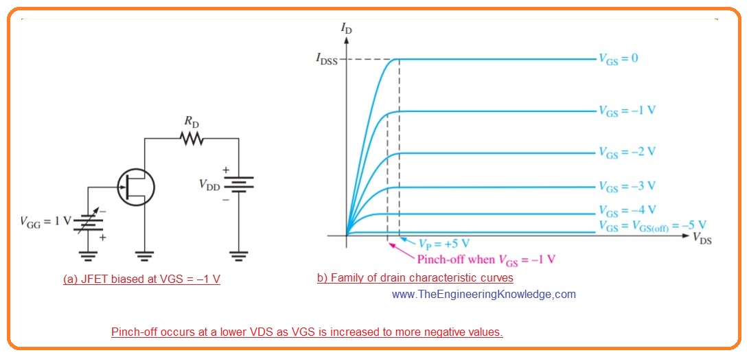
- Note that current ID decreases with the increment in VGS toward negative value due to the area decrement of the channel.
- With that also note that for every increment in VGS, the JFET gets pinch off at the value of VDS less than the VP.
- The condition pinch off is not like to the pinch off voltage VP. since the quantity of drain current is regulated by the voltage VGS it explained in below figure.
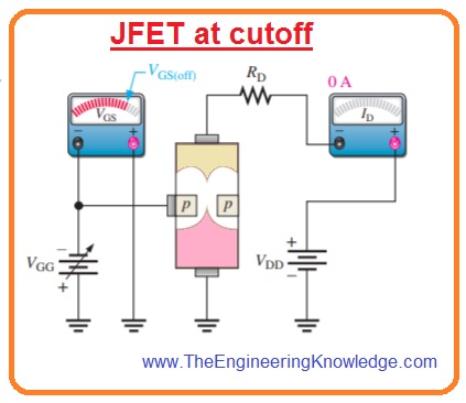
JFET Cutoff Voltage
- The VGS value for which current ID is almost 0 is called cutoff voltage as shown in the above figure denoted as ‘d’.
- The junction field-effect transistor should be a function among the value of VGS=0 and cutoff voltage or VGS(off).
- For these values of gate-to-drain voltages, the current ID will change from the extreme value of IDSS to the least value of almost zero.
- So we can say that for the N channel Junction field-effect transistor large negative value of VGS, there will be a small value of ID in the active region.
- If the value of VGS is a very large negative value than the current ID will become zero.
- This cutoff factor will be caused due to increment in the area of the depletion region to point where it nearer to the channel. It is shown in the below figure.
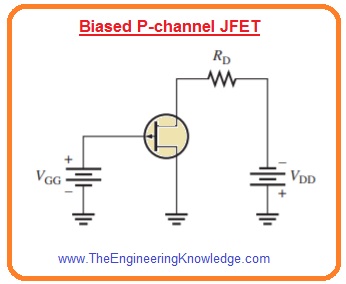
- The main working principle of P channel JFET is similar to the N channel with a difference that the P channel needs a negative VDD and positive VGS as shown in the below figure.
Comparison between Pinch-Off Voltage and Cutoff Voltage
- As we discussed there is a difference between the pinch-off and cutoff voltage the there is some relation both have.
- The pinch-off voltage VP is VDS value at the drain current is constant and equal to the value of IDSS and always calculated at VGSi equal to zero volts.
- Whereas pinch off exists for VDS less than the VP when the VGS is not zero.
- Thus VP is constant the least value of VDS for drain current ID is constant changes with the VGS.
- VGS(off) and VP have the same magnitude but opposite sign.
- The datasheet of JFET has a value of VGS(off) or VP but not both but if you know the value of one second will also known.
- For instance, is VGS(off) is -5 V, then VP will be +5 V.
JFET Universal Transfer Characteristic
- We have discussed that a VGS value range from 0 to VGS(off) regulates the amount of drain current.
- the value of VGS(off) is negative for n channel JFET and positive for p channel JFET.
- As the value of current ID depends on the VGS so relation among these two parameters is significant.
- In the below figure the general transfer characteristic curve is shown which shows the relation among VGS and current ID.
- This graphical representation is asl known as the transconductance curve.
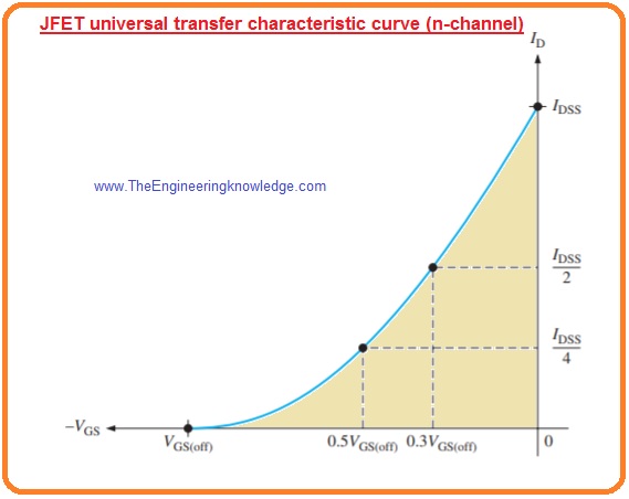
- Note that the lowest part of the curve is at a point equal to VGS(off) at VGS axis and the upper end of the curve at IDSS on the ID axis.
- This graphical representation indicates that.
ID = 0 for VGS = VGS(off)
ID=IDSS/4 for VGS = 0.5VGS(off)
ID = IDSS/2 for VGS = 0.3VGS(off)
- Thus
ID = IDSS for VGS = 0
- The transfer characteristic curve can be created from the drain curve by drawing values of current ID for the values fo VGS taking from the group of drain curve at pinch off as shown in the below figure.
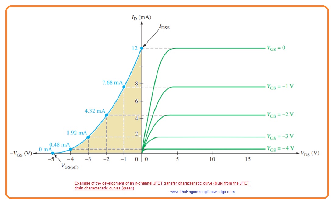
- Every point on the transfer characteristics curve is related to specific values fo VGS and current ID on the drain current.
- For instance for a certain value of VGS(off)=-5 volts and IDSS=12 milliamperes.
- The junction field-effect transistor curve is defined as.
ID=IDSS(1-VGS/VGS(off ))2
- With this above equation, the current ID can be fined for any value of VGS if the values of VGS(off) and IDSS are known.
- These values are normally found in the datasheet of JFET. You can note that square relation in the equation.
- Due to the square expression, the parabolic relation is called square law due to that junction field-effect transistor and MOSFET are also called square law devices.
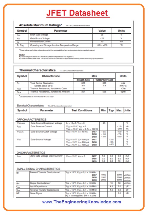
JFET Datasheet
- In the below figure datasheet of JFET is shown.
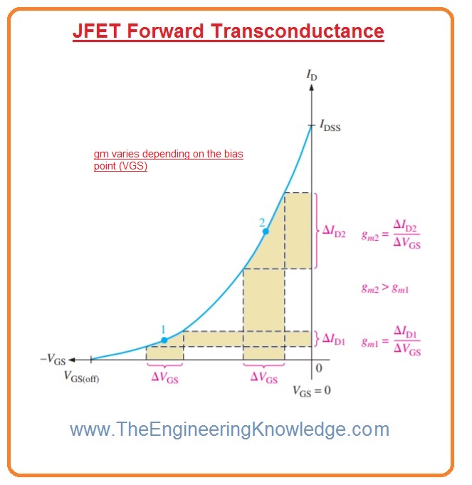
JFET Forward Transconductance
- The forward transducer is also called transfer conductance is the variation in drain current ΔID with the change in the gate to source voltage ΔVGS for a drain to source constant voltage.
- Its unit is Simens denoted as S.
gm=ΔID/ΔVGS
- It can also be denoted as gfs and yfs.
JFET Applications
- These are some applications of JFET.
- It operates as constant curent soure.
- It is used in different circuits as a switch.
- It used as an amplifier.
- It is used as voltage variable resistance.
- It operates as a phase shift oscillator.
Read also
- Common Source JFET Amplifier
- Ohmic Region on JFET Characteristic Curve
- JFET Biasing Method
- Introduction to LF353N Op-Amp
- Introduction to IRLZ34N N-Channel Power MOSFET
That is a detailed post about JFET if you have any questions ask in the comments. I tried my level best to each and every parameter of JFET. Thanks for reading.

bookmarked!!, I really like your blog!
P.S. If you have a minute, would love your feedback on my new website re-design.
Keep up the good work!
Awesome article.
“Having read this I believed it was really informative. I appreciate you finding the time and effort to put this information together. I once again find myself personally spending a significant amount of time both reading and posting comments. But so what, it was still worthwhile!”