 Hello friends, I hope you all are doing great. In today’s tutorial, we will have a look at JFET Biasing Method. The full form of JFET is a junction field-effect transistor. The JFET is a type of field-effect transistor it stands for a junction field-effect transistor. As normal BJT transistor has three terminals called emitter-base and collector. Similarly, there are three terminals of JFET first is a drain, second is gate and third is the source.
The JFET is a voltage control device it used in different electronic circuits and projects as switch and amplifiers. In today’s post, we will have a detailed look at the different biasing methods used for JFET and their relative parameter So let’s get started with JFET Biasing Method.
JFET Self-Biasing Method
- The self bias is commonly used biasing type of junction field effect transistor.
- During operation of JFET the gate-source junction remains reverse-biased condition always.
- For this state the VGS voltage should be negative for N-channel JFET and positive for P channel JFET.
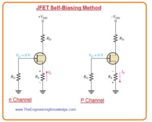
- It can get with the use of self-bias configuration shown in below figure.
- There is no effect of RG on the bias since there is no voltage loss about this resistance and gate also has zero volts about it.
- To maintain zero volts around the gate there is a need of resistance RG.
- For N channel junction field effect transistor as shown in figure denoted as ‘a’ current IS causes a voltage loss about the resistance RS and due to that source is positive with respect to ground.
As IS=ID and VG=0 so VS=IDRS.
- The value of gate to source will be.
VGS=VG – VS=0 -IDRS =-IDRS
- so
VGS = -IDRS
- For P channel junction field effect transistor shown in above figure denoted as ‘b’ the current through RS generates a negative voltage at source terminal causes the gate positive with respect to the source. So IS=ID.
VGS = +IDRS
- The drain voltage with respect to ground can be found as.
VD = VDD – IDRD
- As VS=IDRS, the drain-to-source voltage will be.
VDS=VD-VS=VDD-ID(RD + RS)
Setting Q-Point of Self-Biased JFET
- The simple technique to create JFET bias point is to find current ID for a specific value of VGS.
- After that find the value of RS with the use of given below equation.
- In this equation, vertical lines show absolute values.
RS=ΙVGS/IDΙ
- For a specific value of voltage VGS current ID can be found with the use of two methods. First is through the transfer characteristic curve and the second from given below equation.
ID= IDSS(1-VGS/ VGS(off ))2——-(1)
JFET Midpoint Bias
- Usually, it is favorable to bias junction field transistor at the midpoint of transfer characteristic cure at point ID=IDSS/2.
- For signal conditions, midpoint bias offers the maximum amount of drain current to flow between IDSS and zero.
- From equation denoted as ‘a’ is current ID is half to the IDSS when VGS=VGS(off)/3.4.
ID= IDSS(1-VGS/ VGS(off ))2
ID= IDSS(1-(VGS(off)/3.4)/ VGS(off ))2
- So by using VGS=VGS(off )/3.4 we can get midpoint bias in the form of ID.
Graphical Analysis of Self-Biased JFET
- We use a transfer characteristic curve of junction field-effect transistor and some specific parameters to find the Q point of self-biased circuitry.
- In the below figure dented as ‘a’ circuitry is shown and the transfer characteristic curve is shown in the figure denoted as ‘b’.
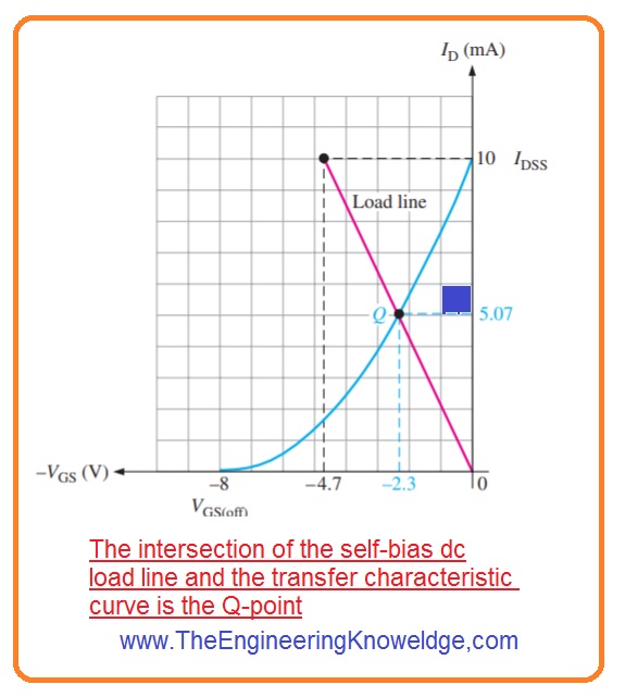
- To find the Q-point of circuit shown in figure ‘a’ the self-biased dc load line is created on the graph shown in the above figure.
- First of all find the VGS when the current ID is 0.
VGS = -IDRS = (0)(470Ω) = 0Volts
- It makes a point at the origin of graph where ID and VGS is zero.
- After that, we find VGS when ID=IDSS from the curve shown in figure denoted as ‘b’.IDSS=10mA
VGS = -IDRS = -(10 mA)(470Ω) = -4.7 V
- It creates 2nd point on the graph which is ID=10mA,VGS=-4.7 V.
- Now with the use of these 2 points, we can construct load line on the transfer characteristic curve as shown in the below figure.
- The point at which load line crosses the transfer characteristics curve is Q point of circuitry as where the value of ID = 5.07mA and VGS = -2.3V.
Voltage-Divider Bias
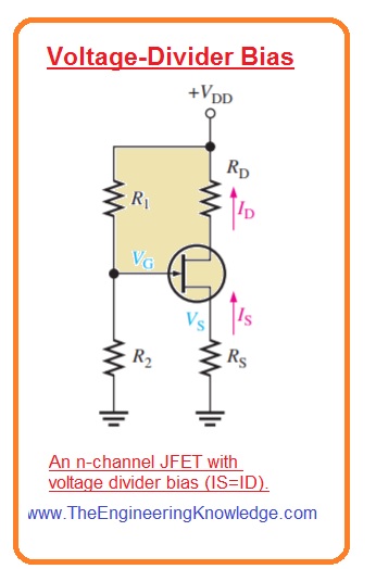
- The n channel junction field-effect transistor with voltage divider bias configuration is shown in below figure.
- For reverse biasing of gate-source junction, there should be the voltage source of JFET should be more positive than the voltage of gate.
- The value of the source will be.
VS = IDRS
- The value of gate voltage is maintained by the resistance R1 and resistance R2 as shown in below equation.
VG=[R2/(R1+R2)]VDD
- The value of gate to source will be.
VGS = VG – VS
- The value of source will be.
VS = VG – VGS
- The value of drain current will be.
ID=VS/RS
- By putting value of RS we have.
ID=(VG – VGS)/RS
Graphical Analysis of JFET with Voltage-Divider Bias
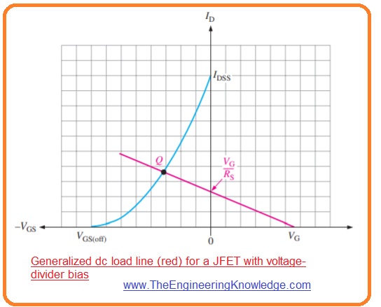
- The technique that we used for self bias can be used for voltage divider bias to find the Q point of circuitry on the transfer characteristic curve in the graphical form.
- In junction field-effect transistor voltage divider biasing when current ID is zero then value of VGS is nonzero which was zero in case of self bias, since the voltage divider generates a voltage at the gate terminal is independent on a current of a drain.
- The load line for voltage divider can be found as.
- If the drain current is zero then.
VS = IDRS = (0)RS = 0V
VGS = VG – VS = VG – 0 V = VG
- So one point on the line at current ID is zero and VGS=VG.
- If VGS =0
ID=(VG – VGS)/RS – VG/Rs
- The 2nd point on the line will be at ID =VG/RS and VGS =0.
- The load line is shown in the below figure.
- The point where the load line is crosses the transfer characteristic curve is called Q point.
JFET Q-Point Stability
- There is a problem that the transfer characteristic curve is different for a different type of JFET.
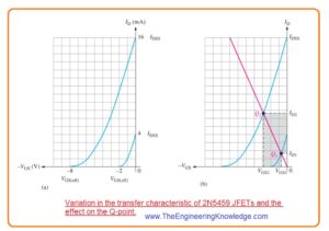
- For instance, if we substitute the 2N5459 junction field-effect transistor with the other 2N5459 transistor the transfer characteristic curve changes also. It is shown in the figure denoted as ‘a’.
- For this condition, the max value of IDSS will be 16 milliamperes and the minimum value of IDSS will be 4 milliamperes.
- Similarly, the maximum VGS(off) -8 volts is and the minimum VGS(off) is -2 volts.
- It means that you have a series of 2N5459 and randomly chose a device its value will be within this above-given range.
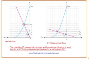
- If we make a self dc load line constructed in the figure denoted as ‘b’ through the similar circuitry with the use of 2N5459 will have Q point on the line from Q1 to minimum bias point to Q2 which is a maximum point.
- So the ID will have a value among point ID1 and ID2 as displayed through the shaded region.
- It means that dc voltage at the drain will have values according to the current ID.
- With that, the value of gate to a source will be among the VGS1 and VGS2.
- The below figure explains the Q point stability for self-biased junction field effect transistor and voltage divider bias JFET.
- For voltage divider bias the dependency of current ID on the value range of Q point decreases since the slope of the load line is less for self-bias.
- Though VGS changes more for both self-bias and voltage divider bias ID has more stability for voltage divider bias circuit.
JFET Current-Source Bias
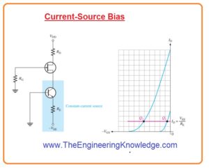
- The current source bias is a technique used to increase Q point stability of the self-biased junction field-effect transistor by making ID independent on the VGS.
- It can be formed by connecting a constant current source in series with the source of the junction field effect transistor. It is shown in the below figure denoted as ‘a’.
- In this circuitry, BJT is operating as a constant current source since its emitter current will be constant if VEE >> VBE.
- The FET can also be used as a constant current source.
IE=(VEE – VBE)/RE
=VEE/RE
- As IE =ID
ID=VEE/RE
- In figure denoted as ‘b’ current ID is constant for any transfer characteristic curve as denoted through the horizontal load line.
What is Pinch Off Voltage
The pinch-off voltage also called the pinch-off point is the voltage over which the drain current of JFET gets saturated and is independent of the drains to source voltage. This happens when the depletion region which is a region of the area about the gate which depleted to charger carriers reaches the source terminal.
This voltage is denoted as Vp and is normally mentioned on the datasheet of JFET. It is important to note that pinch-off voltage not have fixed value, but it changes with gate to source voltage. it is due to the depletion region expansion with the increment of Vgs, that results in decreases in the width of the conducting channel.
The pinch-off voltage is used to measure the transconductance of JFET which is a measurement of how much drain current varies in the result of a change in the gate to source voltage. The equation for transconductance is
gm=Ids/(Vp-Vgs)
In this equation Ids is the drain current, Vp is pinched off voltage and Vgs is the gate to source voltage. The pinch off voltage is the main feature of JFET that can be used to explain the transistor function and measure the operation parameters
So that is all about the JFET bias method if you have any further questions ask in the comments. Thanks for reading.
Read also
- Common Source JFET Amplifier
- Ohmic Region on JFET Characteristic Curve
- Designing High-Frequency PCBs for RF and Microwave Components
- Introduction to JFET (Junction Field Effect Transistor)
- Transistor Symbols | Definition, Terminals & Operating Condition
FAQs
- It defines that FETs are voltage-controlled devices and defines Shockley’s equation and the relation between input and output parameters for different FET types. it defines the three biasing circuits, fixed bias, self-bias, and voltage divider bias
- Biasing is defined as fixed DC voltage or current provided to the terminal of electronic components like diodes, transistors, or vacuum tubes in circuits where AC signals also exist, for establishing accurate operating conditions for the component.
- Drain current in JFET is controlled with changing channel width. Gate source PN junction is reverse biased since if it is forward all channel curent flow to the gate and not the source and JFET can damage.
- JFET is defined as a depletion mode component since they are based on the principle of the depletion region, which is devoid of the majority charge carrier. The depletion region is closed to enable current flow. JFET can come with the n-type or p-type channel.
- JFET is simple type of field-effect transistor.
To avoid these problems, it is good to use the right biasing method for the circuit. It is also important to use high-quality components and to properly design the circuit.
