 Hello, fellows, I hope all of you are enjoying your life. In today’s tutorial, we will have a look at Diode Models. A diode is an electronic device that has 2 terminals positive terminals called an anode and a negative terminal called a cathode. Currently, almost every electronic device use a diode. The main function of a diode is to convert alternating current into DC current. There are such appliances that do not operate on an AC supply as we know in our power system AC is generated and used. So in these devices rectifier circuits are used to convert AC into DC.
If the rectifier converts a full wave of ac into dc then it is known as a full-wave rectifier and if converts half wave it is called a half-wave rectifier. In today’s post, we will have a detailed look at the different diode models compare them with the biasing conditions, and find their parameters. In the previous tutorial, I write a complete post on V-I characteristics of a diode. It will help you to understand the modeling of a diode and diode connection. So let’s get started with Diode Models.
Diode Models
- For circuit analysis and calculation of different diode parameters, mathematical expressions are formed, called diode models, in electronics.
- As we know V-I curve of a diode is not linear for the understanding of the practical behavior of a diode simple circuit model of the diode is needed.
- In today’s post, we will discuss the diode models for ideal and practical diodes and compare them with the detailed.
Diode Bias Connections
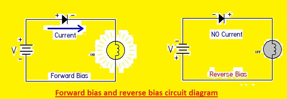
Diode Forward-Bias
- In the given figure, the circuit denoted as (a) shown the forward biasing of a diode.
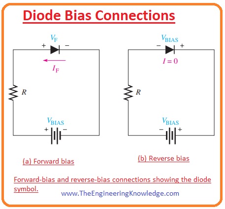
- In this circuit, you can see that the anode of the diode is connected with the positive terminal of the battery and the negative terminal of the battery with the cathode of the diode.
- The resistance between the anode and the battery is used to limit the current to save the value.
- (IF) is the forward current flowing through the cathode to the anode and VF is the forward voltage drop across the diode is equal to the potential barrier of a diode.
Diode Reverse-Bias Connection
- In the above figure, the circuit denoted as (b) shows the reverse-biased connection of the diode.
- In this circuit positive terminal of a battery is connected to the cathode of the diode and the negative terminal is connected to the anode.
- The reverse-biased current is very low and can be neglected and there is no need of limiting resistance in reverse biasing.
- In-circuit you can see that all Vbise or applied voltage is shown across the diode.
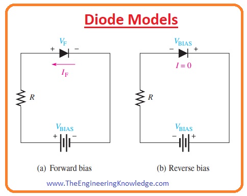
Ideal Diode Model
- In the given figure, the two circuits are shown first discuss the forward biasing ideal diode model and second in the reverse biasing ideal diode model.

- You can see in forward biased condition diode behaves like a closed switch and reveres biased like an open switch.
- In ideal conditions, the potential barrier, dynamic resistance in forward biasing, and reverse current is ignored.
- This model is inadequate for troubleshooting when you are trying to define if the diode is functioning correctly.
- In Figure V-I characteristics of an ideal diode is shown.
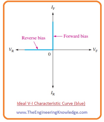
- As the dynamic resistance and potential barrier are ignored the voltage across the diode is zero in forward biasing.
- In forward bias, the curve of an ideal diode is shown on the vertical Y-axis in blue color.
VF =0
- The value of forward current (IF) across the diode can be found by using the value of limiting resistance and biased voltage using Ohm’s Law.
IF =VBIAS /RLIMIT
- As reverses current is ignored in an ideal diode and its value is supposed to be ‘0’. It is shown in the V-I curve on the negative axis.
IR=0A
- The value of reverse voltage is equal to the biased voltage.
VR =VBIAS
Practical Diode Model
- In the given figure there are two circuits shown for practical diode first is denoted as (a) it is forward bias and second denoted as (b) is reverse bias.
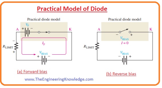
- in a practical model of diode potential barrier is included. In a forward-biased circuit, you can see that the diode is like a closed switch having a series voltage source (VF) equal to the (0.7) volts of its positive side attached to the anode.
- This source is a potential barrier voltage, not a practical voltage source. The value of a biased voltage should be larger to operate the diode.
- While in reverse bias the circuit of a diode is like an open switch and there is no effect in reverse biasing.
- in a given figure, the V-I curve for a practical model of a diode is shown.
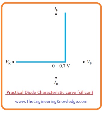
- At a positive X-axis of the diode forward biased condition of the diode is shown in this biasing potential barrier is included so it shown in the graph.
VF = 0.7 V
- The forward current is determined as follows by first applying Kirchhoff’s voltage law to Figure 2–16(a):
- If we apply KVL on the forward-biased circuit denoted as (a) then the value of forwarding current is given as.
VBIAS – VF – VRLIMIT = 0
VRLIMIT = IFRLIMIT
- Now we have.
IF= (VBIAS-VF)/ RLIMIT
- As the reverse current is zero as shown on the negative X-axis of the curve.
IR = 0 A
VR = VBIAS
- For troubleshooting of a less voltage circuit’s practical model of a diode is the best option.
- In this situation, 0.7 volts around the diode can be beneficial and should be taken into consideration.
- Friends if you have to design a basic circuit of a diode then you should prefer a practical diode model.
Complete Diode Model
- Now we discuss the complete model of the diode with diode models in basic electronics that have potential barriers and dynamic forward resistance.
- With these 2 parameters, this complete model also has high-value interior reverse resistance.
- In this model, the reason for reverse resistance inclusion is that this resistance provides a path for the reverse current movement.
- In the given figure, two circuits are shown for a complete model of a diode. The circuit denoted as (a) shows the complete model for forward bias and the circuit denoted as (b) describes the reverse-biased complete model.
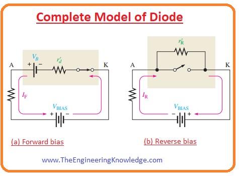
- In forward bias, the condition diode is like a closed switch having a potential barrier (VB) and less value forward dynamic resistance.
- While in reverse biased condition diode operates like an open circuit switch and has reverse interior resistance in parallel.
- In reverse biasing potential barrier is not included as it does not have any effect in this biasing.
- The V-I curve for a complete model of a diode is shown in a given figure.
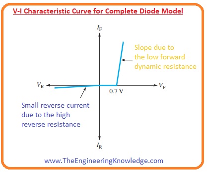
- During forward biasing a potential barrier and dynamic resistance is included so there is (VF) forward voltage across diode exits.
- The voltage (VF) will be equal to the sum of the potential barrier voltage and the voltage drop across dynamic resistance. This voltage is shown on the positive X-axis in the curve.
- The graph in forward bias is like a slope due to an increment in a voltage drop across the dynamic resistance with the increase in current.
- The given below mathematical expression is for a complete model of a silicon diode.
VF = 0.7 V + IFr’d
IF = (VBIAS – 0.7 V)/(RLIMIT + r’d)
- During reverse biasing reverse current IR is taken into consideration and shown on the negative X-axis of the curve.
- On this curve breakdown region of the diode is not shown as it does not save the operation region for some diodes.
- Due to the complex calculations, the complete model is not suitable for troubleshooting of diode.
- The complete model can be used when the computer is used to solve complicated calculations.
Forward bias and reverse bias circuit diagram
forward bias and reverse bias circuit diagrams can seen here
Related Posts
- Current Regulator Diode
- Zener Diode
- Step Recovery Diode
- PIN Diode
- Schottky Diode
- Photodiode
- Varactor Diode
- Diode
- Zener diode Applications
- Laser Diode
- LED


Hi to all, how is the whole thing, I think every one is getting more from this web page,
and your views are pleasant in support of new people.
I read this article fully about the resemblance of most recent and earlier technologies, it’s remarkable article.
My brother suggested I might like this web site. He was entirely right.
This post truly made my day. You cann’t imagine just how much time I had spent
for this information! Thanks!
I know this if off topic but I’m looking into starting my own blog and was curious what all is needed to get set up? I’m assuming having a blog like yours would cost a pretty penny? I’m not very internet savvy so I’m not 100 certain. Any tips or advice would be greatly appreciated. Thank you
Hello, i’m an EEE student currently studying semiconductor.
Are the currents provided in the model-diagrams above based on “electron’s direction” as opposed to “conventional current direction”?
I’m fairly new to the concept of electricals, it’d be really helpful if you could clarify this for me.
Thank you in advance.