
Hello readers welcome to the new post. In this post, we will have a look at The Importance of Copper Pour in Empty Areas on PCBs. Copper pours are commonly used design of printed circuit boards. it has empty filling areas on boards with copper planes that offer differnt advantages for electronic projects. In this post, we will cover different parameters of copper pour and its effect on board performance. Let’s get started with Introduction to Copper Pour
Introduction to Copper Pour
The desing of PCB board engineers works on the board operation, reliable nature, and functions. The copper pout is a technique that is helpful to use empey points of the board to increase their working. The killing of these empty points with the use of copper plans, designers and engineers manage heat dissipation reduce effect of EMI, and increase signal quality
What is Copper Pour on PCBs?
Copper pours is the process creation of larger areas of copper planes on PCb boards. These planes are connected to ground or power planes covered with empty areas between traces and components. This pout is applied on inner layers of board with that also used on external layers
Why is Copper Pour Important?
Enhancing Heat Dissipation
The main benefit of making copper pout on board desing is features to increase heat dissipation. The heat generated by active components can be moved through copper planes and spread on the baord. It avoids the creation of hotpots and ensures good operating temperature for the component connected
Reducing Electromagnetic Interference (EMI)
These pours also reduce the EMI on board. The copper plans provide protection minimizing the EMI effect on components and traces of boards. It reduces cross-talk signal degradation and noise and increases the overall operation of the system
Wholesale PCBs SMT Stencil & PCBA Service Provider
Special offer:$2 for 1-8 layer PCBs
Copper Pour Design Considerations
The weight of the copper is an important account desing of the board. High copper weight can have good dissipation and current carrying features they increase the production cost and cases of etching issues.
Clearance and Spacing
Clearance and spacing for copper pour are areas that prevent undesired shorts or signal interference. Accurate clearances should be done between a copper pout and components an signal lines.
Shape and Placement
The structure and connection of copper pours must be accurately configured. Irregular copper pout can cause heat distribution or EMI shielding fautls. Designer must make a balance between copper pour desing to increase advantages while reducing faults
Benefits of Copper Pour
Thermal Management
They effectively dissipate heat on boards offering good temperatures for components. Reducing hotpots and making a balance between thermal layout copper traces increases the operating life and reliability of devices
EMI Shielding
The continuous copper planes are a protection to minimize EMI of the board that offers good signal quality and reduces noise and good overall operation of the system
Voltage Distribution
Copper pours maintain regular volts over the board and reduce voltage losses and ensure stable power to components
Signal Integrity
Through offering low impedance paths copper pours increase the quality of the signal. It reduces signal reflection, attention, and crosstalk and he’s reliable for data transmission
Copper Pour Techniques
Solid Copper Pour
In this copper pour technique, empty areas on boards are filled with continuous copper planes. That offers the highest heat dissipation, EMI protein, and signal quality increment, But it is not good for design due to the high cost
Hatched Copper Pour
This technique is used to make grid-like patterns in the copper pour areas leaving small gaps between copper traces. This process involves a balance between heat dissipation and production gaps between copper traces. it makes a balance between heart dissipation and production parameters. It is used for proper copper pouring reducing features and materials cost
Thermal Relief Pads
It is a copper connection used to have isolation between copper planes and surface mount components. These pads decrease heat flow from component to copper pouts and provide good soldering
Copper Pour in Different Applications
High-Speed PCBs
In high-speed boards the signal quality is important. The copper pour minimizes signal distortion and reflection crosstalk and makes sure reliable data transmission in high-frequency circuits
Power Electronics
In power electronic circuits heat is produced. COpper pous reduces heat dissipation offers reliable operation and increases circuit life
RF and Wireless Communication
RF and wireless communication circuits require control for signal quality. The copper pour minimizes interference singal losses and provides good RF operation
How Does Copper Pour Affect Crosstalk and EMI?
- Crosstalk Reduction:
- Porus minimizes crosstalk by having a protection layer between sensitive signal traces. It covers traces with copper pours electromagnetic field generated by traces can be attenuated. it reduces coupling signals between neighboring traces and reduces crosstalk.
- Ground Plane:
- Ground plans arranged with copper pours can provdie differences for low impedance for return path in signals. it helps to reduce loop areas of high-speed signal that decreases the returning path for signals. it Ground planes also provide stable reference voltage and reduce ground bounce
- Impedance Control: It can also control features of the impedance of transmission lines. Through adjusting the width and copper pours placement tune of impedance matches the needed value. it reduces signal reflection and increases signal quality
- EMI Shielding: it can work as a good protector for EMI. Covering components or traces in copper pour it can reduce cooling of the outer electromagnetic field and
- Grounding Considerations:
- Coper pours can be good goog grounding and copper pours can be used for required results. If copper pours are not correctly connected to solid ground plane can cause ground loops to increase EMI
- Parasitic Capacitance and Inductance: copper pours cause parasitic capacitance and inductance in the board. It can affect signal and result in signal degradation and crosstalk problems.
Copper Pours vs Ground Pours
| Feature | Copper Pours | Ground Pours |
|---|---|---|
| Purpose | conductive area for copper traces or components | it offers fewer impedance paths returning paths |
| Signal quality | it has an effect on signal quality for high-speed traces | it reduces inductance and noise increases signal quality |
| EMI/EMC | Not have good EMI/EMC benefits | it is good for EMI/EMC |
| Power Distribution | Not used for power distribution | it used for power distribution |
| Controlled Impedance | affect impedance control for high-speed traces | It helps to get controlled impedance for signal traces |
| RF and High-Frequency | Not used | good and uses |
| Thermal Management | Not used | uses |
| Ground Reference | not have a stable ground reference | have a stable ground reference |
| Design Flexibility | design flexibility and routing options | not provdie |
| PCB Real Estate | copper traces or components | For ground plane |
Importance of Copper Pour in Empty Areas on PCBs & Notes on Using Copper Pour
In a PCB design, too much-unused space without copper can have a detrimental impact on production and the caliber of the finished product. Filling empty space on a PCB board with planar copper is called placing copper pour. All significant PCB design software has the ability to automatically insert copper pour, which is an important component of PCB design. Copper pour decreases ground impedance, boosts power efficiency by minimizing voltage drops, and minimizes EMI by reducing loop regions, all of which contribute to the development of EMC.
JLCPCB produces high-quality PCBs in five independently owned intelligent manufacturing bases employing cutting-edge machinery and raw materials. All PCB manufacturing linkages are under the good control of JLCPCB.
Outer Layer copper pour: 2- and Multi-layer Boards
Boards are put in a plating solution and electroplated with a fixed current after a dry coating has been applied to them.
Unused areas left blank
Under the influence of the current, exposed copper that is not covered by the dry film will increase in thickness from copper in the solution.
Unused areas filled with copper pour
The amount of exposed copper during this procedure will have an impact on how the current is distributed. Large copper pours are advised in PCB designs because they allow for more uniform current distribution.
Imaged PCBs ready for electroplating
Under the influence of the current, exposed copper that is not covered by the dry film will increase in thickness from copper in the solution.
PCBs undergoing electroplating in an electrolyte bath.
The amount of exposed copper during this procedure will have an impact on how the current is distributed. Large copper pours are advised in PCB designs because they allow for more uniform current distribution.
Large areas of copper exposed for plating
On the other hand, if the exposed copper portions on the PCB are tiny or not equally spaced out, they will experience varying currents and subsequently have varying plating thicknesses, with a larger current producing a thicker plating. A supposedly 1 oz board may contain 2 oz of copper thickness as a result of this.
Not enough copper exposed during plating
The chemical process of electroplating
Electroplating causes two traces with very little separation (e.g., 4 or 5 mils) and no surrounding copper to thicken to the point that the dry film between them is challenging to remove prior to etching. As a result, extra copper accumulates between the traces, perhaps resulting in short circuits.
Dry film remains between two closely spaced traces
Solution
To assure the quality, try to minimize the number of “standalone” traces in your design and distribute the copper pour as evenly as possible over the board. Design the spacing between the traces as large as feasible if part of the “standalone” traces can’t be set with the copper pour. The designs that are problematic and their better iterations are shown in the examples below.
Copper pour has only partial coverage:
Before Improvement
After Improvement
No copper pour at all:
Before Improvement
After Improvement
Inner Layer copper pour: Multi-layer Boards
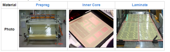
Cutting the prepreg to the proper size, sandwiching it between two core layers or one core layer and one copper sheet layer, and then applying high heat and pressure to the assembly to melt and cure the prepreg’s resin, which bonds the layers together, are how multi-layer PCBs are laminated.
Prepreg
Inner layer core
Laminate
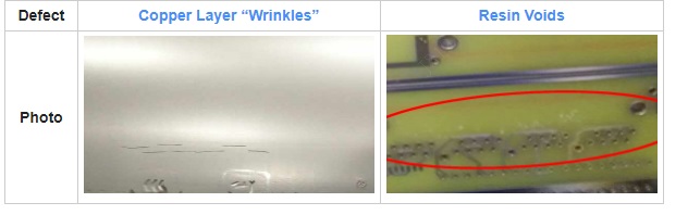
1) Resin on the prepreg will need to extend out to cover the copper-free zone if a copper layer contains significant blank regions. This may result in layer separation, voids in the resin, folds and creases in the copper, and PCBs that are thinner than typical.
A fold in a copper layer
Voids in a resin layer, visible from the white marks
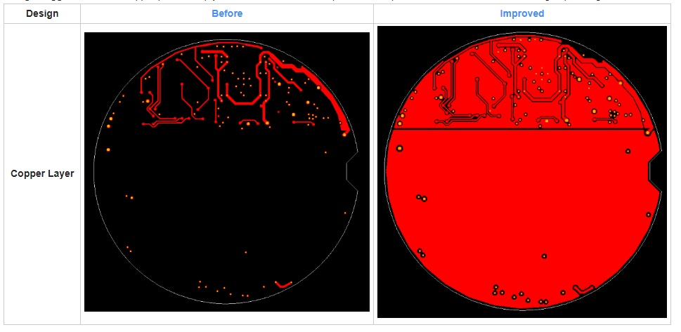
Design example:
Before Improvement
After Improvement
2) The Goldfinger region will be narrower than intended if the inner layer area of the Goldfinger is highly empty. This might result in poor contact between the PCB and the matching connection slot, among other problems.
1.6 mm nominal, 1.41 mm measured
Before: no copper pour in inner layer area of the goldfingers
After Improvement
For PCBs with gold fingers:
Because the inner layer region of the Goldfinger has greater thickness restrictions, copper pour must be put there. When ordering, be sure to choose a stack-up with a nominal finished thickness that is suitable and stay away from stack-ups whose thickness is close to your acceptable lower limit.
The topic regarding utilizing copper pour notes is below. In order to assure the consistency of lamination and the thickness tolerance of the completed board, copper is typically poured into the empty space of the inner layer of multi-layer boards. This increases the copper area and decreases the resin spread-out area. The major goals of the copper pour in the vacant region of the outer layer are to uniformly distribute the electroplating current, reduce the chance of short circuits and thin lines brought on by over-etching, and prevent these problems.
Use Thermal Relief Pads Within copper pour
Copper has a thermal conductivity of about 380 W/(m K). Because of this, if a pad is completely attached on both sides to the copper plane next to it, soldering problems will result from heat dissipating away too rapidly. The use of “thermal relief” pads lowers heat dissipation and facilitates soldering.
Hatched and Solid copper pour
As is well known, high-frequency situations cause the dispersed capacitance of the traces on a PCB to become important. When a trace’s length exceeds one-twentieth of the noise frequency’s wavelength, the trace turns into an antenna and radiates the noise into the surrounding area. Any copper pour that is not properly grounded will contribute to the noise’s subsequent propagation. As a result, ground connections in high-frequency circuits must not only have electrical continuity but also be spaced apart by less than 20. Vias on traces can assist in multilayer boards’ “good grounding” to the ground plane. Copper planes that have been properly constructed boost current capacity while also lowering EMI.
Solid and hatching are the two main types of copper pours. Solid pours enhance current capacity and offer to shield, but when wave soldering is used, they can lead to copper separation and warping. Designing holes or apertures into solid copper pour helps to ease this. Hatched pours, on the other hand, primarily serve as shielding and have a low current carrying capacity.
Hatched pours may help to dissipate heat since they have less copper surface area. Hatched pours do have one drawback, though the copper “segments” they are made of can increase electromagnetic interference (EMI). If the electrical length of the operating frequency of the circuit is close to the length of these segments, the circuit may not function at all because the entire pour acts as many antennas transmitting interference signals. It is important to match the copper pour type to the PCB circuit; for high-frequency circuits with EMI requirements, use hatching pours; for low-frequency or high-current circuits, use solid pours. All major PCB manufacturers have switched from the inferior wet film technique to the superior dry film process since new PCB designs need more accuracy and quality. It is advised to utilize solid pours rather than hatched ones whenever feasible since hatching copper pours can cause the film to shatter when used with dry film procedures.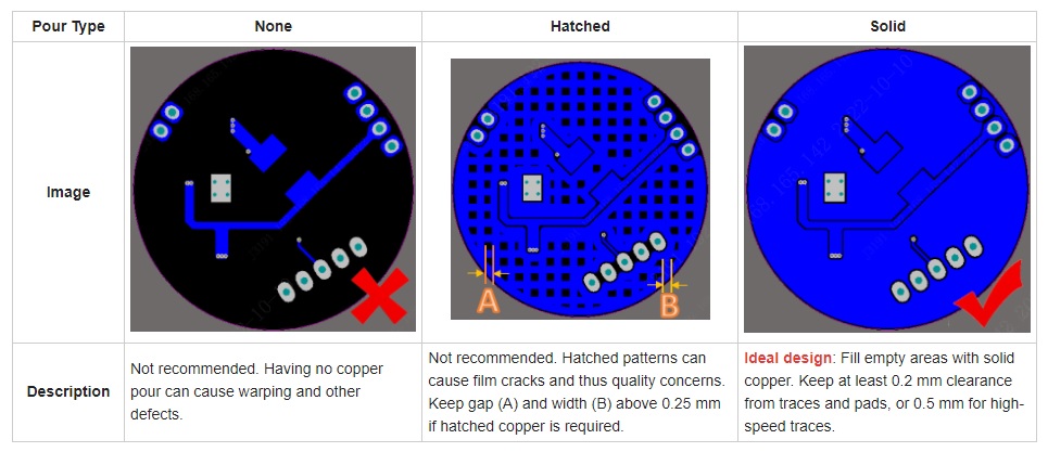
Copper Fills on Inner Layers
Copper coverage: the amount of copper that is still on an inner layer after etching in relation to the size of the entire board.
Laminating: Prepreg is measured, trimmed to size, and sandwiched between inner layer cores or between a copper sheet and a core. The prepreg layers’ resin component is melted by heating and pressurizing the layered stack (laminate). When the resin is cooled, it flows to fill any copper-deficient regions on the next layers and fuses them together.
Design issue:
Because the inner layers of the prepreg have less copper coverage, the additional resin needs to be stretched out to fill the copper-free area. A thinner board than anticipated, folds or creases in the copper layers, voids in the resin, and maybe layer separation owing to a shortage of resin are all consequences.
Design suggestion When feasible, pour copper where there are voids on the board. Maintain a 0.5 mm distance between your device and high-speed signal traces.
Calculating Total Laminate and Finished Board Thickness
Core + cured prepreg + outside copper = theoretical laminate thickness
= (0.7×2) + (4.54+4.48) + (1.2+44.84+1.2) = 57.66 mil = 1.46 mm.
Theoretical board thickness is comprised of the core, prepreg, and solder mask.
= (1×2) + (1.4×2) + (4.54+4.48) + (1.2+44.84+1.2) = 61.06 mil = 1.55 mm.
when the neighboring core layers’ resin-filled thickness and the cured prepreg thickness are equal.
= (Thickness of copper covering divided by the thickness of uncured prepreg)
The table below describes a sample stack-up.
Using layers 1 and 2 as an illustration:
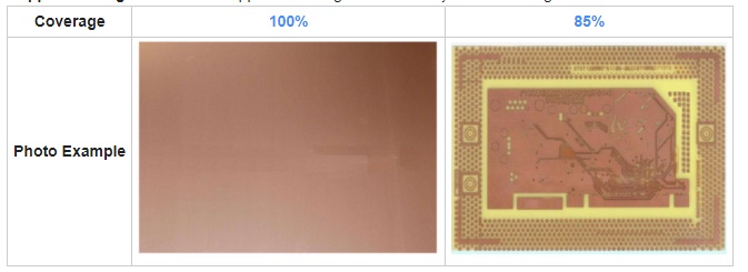
– Inner layer copper weight is 1 oz, layer 2 copper coverage is 85%, uncured prepreg thickness is 4.72 mil.
– Thickness of the cured prepreg is 4.72 mil minus ((1 – 85%) 1.2) = 4.54 mil.
The actual thickness of one ounce of copper is 30 micrometers (1.2 mil), despite the fact that the nominal thickness of one ounce of copper is 35 micrometers.
Design Guidelines Summary
1. Don’t leave any PCB space that lacks copper empty. Pour copper in the spaces.
2. If copper pouring is not practicable, traces should be built with a least 8 mil (trace to trace, trace to pad, pad to pad) spacing and a 2-ounce copper weight.
3. The copper pour should have more than 0.5 mm of space between it and the working traces and pads. Avoid employing hatching copper designs, particularly those with small grid sizes; opt instead for solid pours.
4. To prevent an inadequate board thickness, copper pour must be present in all of the inner layers of gold fingers. Avert stack-ups with completed thicknesses that are too thin.
5. To prevent obstructing the operation of PCB antennas, the copper poured around them should be built in accordance with specified product specifications.
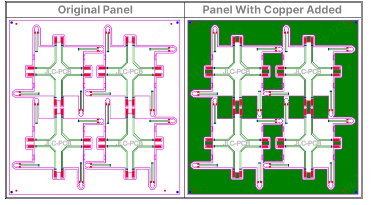
Note: The importance of JLCPCB adding copper pour
In order to prevent faults brought on by wide empty areas, such as low board thickness and uneven plating, JLCPCB may add copper pour to panels on both the inner and outer layers of multi-layer PCBs. Only handling strips, bridge components, and other places outside PCB units will receive a copper pour. The practical PCBs will not contain any more copper. Around fiducials, mechanical holes, mouse bites, and V-cuts, clearance will be added.
JLCPCB continues to work towards giving consumers a larger option of PCB fabrication since it sees pushing technological progress as its responsibility. Not only that, but JLCPCB also offers complete PCBA services, including buying high-quality PCBs, locating 1,000,000+ authentic electrical components, and assembling your PCBs using cutting-edge SMT equipment. Join JLCPCB today to receive up to $54 in new user discounts and to begin your PCB adventure!