 EMI stands for Electro Magnetic Interference also referred to as radio frequency interference. It is disruption created by some outer causes which have an impact on electronic circuits due to electromagnetic induction. EMI has reduced the operation and reliable behavior of the circuit where it works. To make circuit boards efficient there must reduce this fact during PCB construction.
For data path, EMI can range from the increment in fault rate to net losses of data. Human and natural causes produce electrical current and voltage that resulted in the EMI like mobile communication systems, ignition systems, lightning, solar flares, etc. EMI normally disturbs the AM radio signals. That also has a bad impact on mobile phone signal transmission, FM radio, TVs with that atmosphere science.
EMI is caused due to interaction of electricity and magnetism. Every electrical flow causes a small magnetic field. As a result, the moving magnetic field causes a current. On these principles, motors and generators operate. So all electric conductors can function as radio antennas. High-power electrical and radio signals have bad effects on different electronic circuits. As electronic circuits are small size high speedy and compact so they become sensitive to these effects that produce the EMI
How EMI Produced
EMI is not a good factor for different electronic devices to operate well. Since PCB is used in different medical instrument circuits and military operations so they must have less faults to operate well. So engineers take such precautions to avoid these issues. Some factors produce the EMI that must know to reduce EMI from circuits
Inaccurate PCB design
If the design of PCB boards is not configured properly there must be some signal not moving in the circuits and causing interference resulting in EMI. Make sure that there is sufficient grounded plane connected with every component connected on board.
With that have effective trace paths that avoid the radiation of EMI. For this bend traces to larger than forty-five degrees at one point.
Bandwidth
Broadband interference affects the larger data signal transmission. While narrowband signals can affect a certain part of the bandwidth.
Impulse Interference
Periodic impulse interference created by lightning and non-certain sources causes problems in the circuit to transmit signal
Environmental Conditions
Different environmental conditions like lighting create EMI problems in boards.
How to Reduce EMI in PCB Boards
The process used to remove the EMI in PCB boards is discussed here

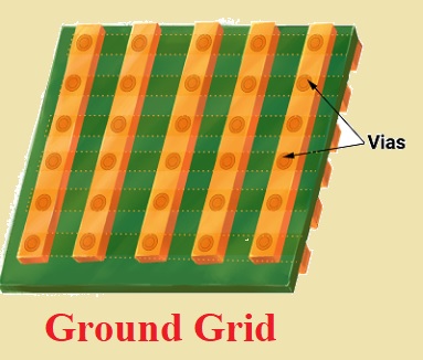
Ground Plane
The electrically conductive surface connected with the electrical ground is called the ground plane. For PCB boards ground plane is created through the use of a copper layer. That is connected with the power supply ground point and provides the return path for current from different elements and parts of the circuits connected on board. If you have a larger size of ground plane there is will be fewer issues of electrical noise, interference due to ground loops, and crosstalk in circuits. When digital circuits change their state current pulses will pass through devices to the ground point. The high impedance will cause high voltage losses, which will produce a larger noise. By providing a high conducting area, interference can be decreased. Some other techniques for enhancing the operation of ground planes are
Applications of multiple layer board
Use of split ground
Connect the split ground plans with a single connection
Trace Layout
The other method to avoid the EMI in PCB boards is to use a trace layout. The traces are conductive paths. If circuits are active they consist of electrons. The bending of the trace layout can cause the creation of an antenna. For the creation of trace, layout follow some rules
Minimize the charge angle bends
Make separation among the signals
Make return paths smaller
There must be partitions among the high-speed components
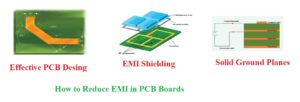
EMI Shielding
EMI is generated in numerous devices. To reduce its bad effects on circuits, there is not to enhance the electromagnetic compatibility, or circuit design configuration to face fewer faults in circuits through the use of shielding. By applications of shielding, we can protect the receiver from having outer electromagnetic signals or avoid high signals having an impact on different electronic components. The use of EMI shielding coating can save different PCB components like connectors and cables among the PCB boards.
A good PCB shielding process can be obtained if we use a dual-fire process and deep coating.
Types of EMI
The main types of EMI are discussed here
Narrowband EMI
Broadband EMI
Narrowband EMI that caused by the transmission signals of radio, TV, and cell phones.
Broadband EMI that used by the electrical power transmission lines’ radiations
Conducted electromagnetic interference is produced due to the physical connection between conductors that create hindrance for EMI produced by induction. Electromagnetic disturbances in the electromagnetic field of conductors will not be retained on the surface of conductors and will spread. It will continue in all conductors and mutual inductance among the two electromagnetic fields will cause EMI.


