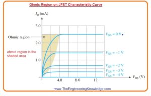
 Hello friends, I hope you all are doing great. In today’s tutorial, we will have a look at Ohmic Region on JFET Characteristic Curve. The ohmic region of JFET is a region at which drain current shows linear behavior for variation in the drain-source voltage. This behavior is like to the ohms law so called ohmic region. The value of ID depend on the drain-source voltage VDS. At starting point when the value of VDS is less drain current increase in direct relation with the VDS.
If JFET is properly biased in ohmic region it behaves like a variable resistance at this point value of resistance is regulated by VG. In today’s post we will have detailed look at ohmic behavior of JFET and its effect on characteristic curve. So let’s get started with Ohmic Region on JFET Characteristic Curve.
Ohmic Region on JFET Characteristic Curve
- The ohmic region starts from the origin of the characteristics curve to the point from active region start where VGS=0 it shown in below figure.
- In ohmic region, characteristic curves are have almost constant slop for a small value of drain current ID.
- The slope of JFET characteristic curve in the ohmic region is dc drain to source conductance GDS of junction field effect transistor.
Slope=GDS=ID/VDS
- As we know that resistance is inverse of conductance.
- So dc drain to source resistance is mentioned here.
JFET as a Variable Resistance
- The biasing of JFET can be done by the through the active region or by ohmic region.
- If JFET operating as voltage control variable resistance it biased in ohmic region.
- The control voltage are VGS and it find resistance by changing the Q-point.
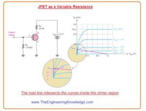
- For JFET biasing in ohmic region, the dc load line should intersect JFET characteristic curve in the ohmic region as shown in the below figure.
- To perform this in such a way that permits VGS to regulate the value of RDS, the value of dc saturation current is less than the IDSS so the load line meets most of the point of the characteristic curve in the ohmic region as explained.
- For this condition.
ID(sat)=VDD/RD=12V/24kΩ=0.50 milliAmperes
- The above figure denoted that the operating region extends with 3 Q points first is Q0, second is Q1, and third is Q3 which depends on VGS.
- If we move along the load line within the ohmic region of above figure the value of RDS changes as the Q points decrease largely on the curves with changing slopes.
- The Q point is moving with the load line changing from VGS zero to VGS=-2volts.
- After that occurrence, the slop of the slope of every succeeding curve is less than the preceding one.
- The decrement in the slope of corresponds to lesser drain current and larger VDS that infers an increment in resistance RDS.
- This variation in resistance can
- This change in resistance can be used in numerous applications voltage regulation of resistance is beneficial.
Q-point at Origin
- In some amplifiers, we have to very resistance observed by the ac signal without changing the dc bias to control the gain.
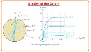
- In some cases, JFET is used as a variable resistor in a circuitry where bot current ID and voltage VDS are zero that mean Q point is at origin.
- The Q point at origin is obtained with the use of capacitor in the drain circuitry of junction field-effect transistor.
- It causes the dc parameters VDS =0 and drain current ID=0milliampere, so the only variable parameters are VGS and drain current Id.
- At origin we have ac drain current regulated by the VGS.
- As we know that transconductance can be defined in drain current for resultant variation in the gate to source voltage.
- So for biasing at origin main point is transconductance. The below figure shows the characteristic curve at origin.
- You can note that the ohmic region is a move to the 3rd quadrants
- At the origin when VDS=0 volts and ID is zero milliamperes the equation for transconductance is given as.
gm=gm0(1-VGS/ VGS(off))
- In this equation, gm is transconductance and gm0 transconductance when VGS=0.
- gm0 can be calculated through this equation.
gm0=2IDSS/|VGS(off)|
FAQS
What is the ohmic region in JFET?
- The region where the transconductance curve has a linear response and drain current is opposed through transistor resistance is called the Ohmic region.
What is the difference between the saturation region and the ohmic region?
- Ohmic is a region where ID is a function of vGS and VDS. Id increases linearly with VDs, so it is known as linear. Saturation is a region part of the constant ID, defined with VGS-VT. In the saturation region, ID is not affected by VDS.
In which region does JFET act as a resistor?
- It comes with a triode region and a saturation region. In the triode region, JFETs work like a resistor, but in the saturation region, they work like a constant-current source.
That is a detailed post about Ohmic Region on JFET Characteristic Curve if you have any questions ask in comments. Thanks for reading. Have a good day.


