 Hi, friends welcome to the new post. In this post, we will have a detailed look at Transistor Symbols. The transistor is a miniature semiconductor device that regulates curent or voltate flow for amplifier and prodcues electrical signal working as switch/gate for them. In this post, we will cover the details of transistors, working, definition, and other parameters. So lets gets started with So let’s get started with Transistor Symbols.
What is a transistor?
- The transistor comes with 3 layers or terminals of semiconductor material, and each layer carries current. The transistor is created with the use of 3 layers that are called the emitter, base, and collectors. The signal is given of base and curent flow between the emitter and collectors of the transistor.
- Bipolar junction transistors (BJTs) and field-effect transistors (FETs) are two basic types of transistors. Every transistor comes with a symbolic representation that is best to find the transistor for any use.
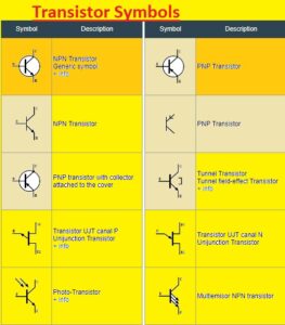
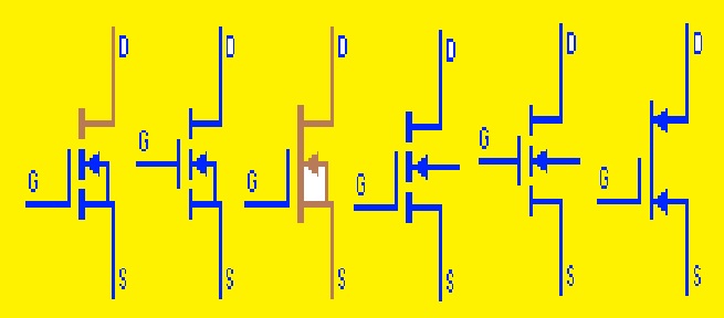
Transistor Symbols
- Each transistor has its own symbol and differentiates from other transistor.
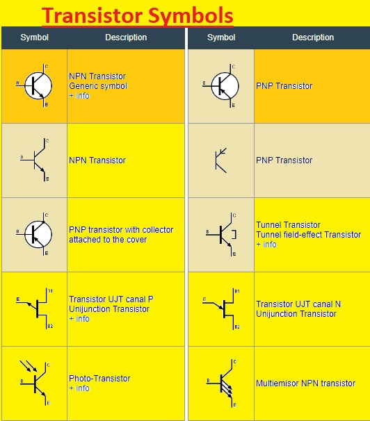
Bipolar junction transistor (BJT) symbol
- BJT or Bipolar junction transistors is simple transistors that are used very comonly. It has three terminals collectors, based and emitter here the symbol of BJT or Bipolar Junction Transistor. BJT has two types based on structure NPN and PNP
Related Topics
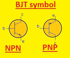
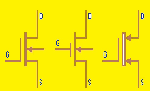
A field-effect transistor (FET) symbol
- The field effect transistor is a transistor type that uses electric field to control the current flow in the semiconductor. it has two types JFET and MOSFET. FET has three terminals source, gate, and drain.
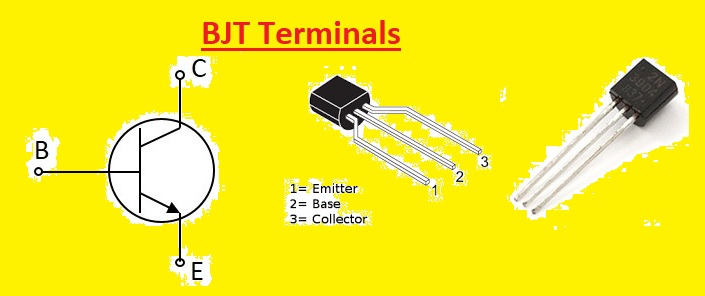
Terminals of Transistor Symbols
BJT terminals
- BJT has three terminals, emitter, base, and collectors. Power source positive terminals connected with collectors and negative with the emitter. Base operates for control an regulation flow of current in transistors circuit
FET terminals
- The FET has 3 terminals that are source, drain and gate. The source is terminals where the majority of charge carriers goes in FET. Drain terminals help charge carriers to exit from FET
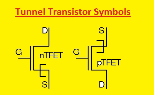
Tunnel Transistor Symbols
- TFET or Tunnel Field effect transistor is a MOSFET transistor type that has a structure like the conventional MOSFET, with a different switching process. it uses the phenomena of quantum tunneling that make best for lower power electronics.
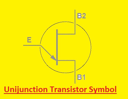
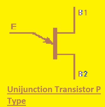
Unijunction Transistor Symbol
The emitter, base 1, and base 2 are three terminals of in junction transistor. Base 2 is with line that connects base 1 and emitter through diagonal line connected with B1
The UJT symbol is here
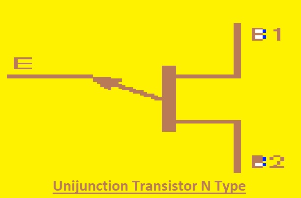
Unijunction Transistor N Type
Unijunction transistors are created with the use of less doped base with a heavily doped emitter making a single junction. It is also called a double-base diode. The potential at emitter according to base controls current through base. N-type UJT is created with a less doped P-type base with a heavy doped N emitter. it is used for triggering thyristors.
Unijunction Transistor P Type
It is P-type junction transistor made with bar of less doped N type material heavily doped P material close to the base 2. it works like N N-type UJT with voltge polarity reversed.
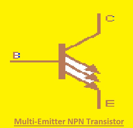
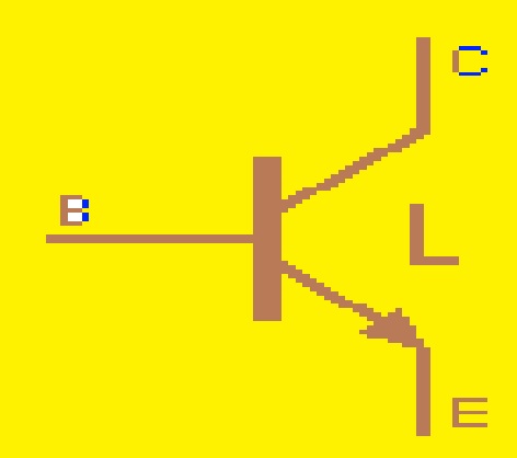
Multi-Emitter NPN Transistor
It is special BJT type that comes with multiple emitter. The emitter is independent of each other and current through every emitter based on the individual voltae according to the base of the transistor. it used in TTL NAND gates.
Schottkey NPN Transistor
It is made of a Schottky diode and a transistor. The Schottky diode is connected between the base and the collector. It maintains the transistor from saturating through a shunt high current. It helps in fast switching due to the time delay for removing stored charges in saturated mode.
![]()
JFET Transistor N channel
JFET or junction field effect transistor is a unipolar transistor since current flow is due to one carrier. JFET is voltage-controlled, or current flow is regulated through voltage at the gate terminal. Voltage increases or reduces the depletion region, controlling current flow. The N-channel JFET comes with an N-type channel between the source and drain and the gate is created with P-type material.
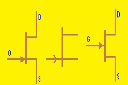
JFET Transistor P channel
In a symbol of P channel JFET is denoted with an arrow pointing outwards. The P channel JFET is created with the use of P-type channel between the D and S pins and the gate is made with N material. P channel JFET switches off by maintaining a positive gate to source voltage.
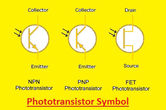
Phototransistor Symbol
- The phototransistor comes with a basic bipolar transistor symbol with 2 arrows directing to junction of bipolar transistors.
The photo-transistor symbol is here
Avalanche Transistor Symbol
The avalanche transistor is a bipolar junction transistor made for working in the region of collector current voltage features beyond the collector-to-emitter breakdown voltage, known as avalanche breakdown region.
NPN Darlington Transistor Pair
it is a special transistor created with a connecting emitter of one BJT to the base of another BJT for increasing current gain and sensitivity. It can be created with an NPN or PNP transistor through the connection shown in the figure. The total gain of the Darlington transistor is multiple of gains individual BJT and the voltage loss is double at the base-emitter.
Sziklai Transistor Pair
This transistor is made with use of two NPN and PNP transistors in the Darlington pair structure. The main benefit of this design is that switch on with 0.7 volts and total gain is the same Darlington pair.
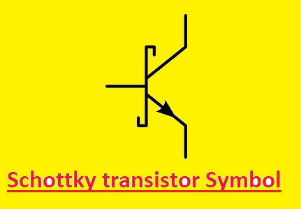
Schottky transistor Symbol
- The symbol of the Schottky diode is different from the PN junction diode symbol. The cathode line is like the symbol S. The current is measured through a diode anode to a cathode. The voltage of the diode is measured from anode to the cathode. Cathode is S like shape.
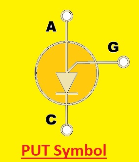
PUT Symbol
- PUT or programmable UJT is 4 NPN layer devices like thyristors but it operates like UJT if programmed with 2 external resistors. it has an anode, cathode, and gate terminals. The voltage at gate terminals switches PUT on and off during crossing the cutoff level
The PUT symbol is drawn here
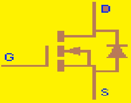
Depletion Type MOSFET
Metal oxide semiconductor FET is a field effect transistor whose gate is isolated from the current-carrying channel so it is known as IGFET. It is voltage voltage-controlled current device. The depletion MOSFET is normally ON at zero gate-source voltage. it switches off by applying positive or negative gate-source voltage for P or N channel MOSFET respectively.
Enhancement Type MOSFET
The E MOSFET does not normally conduct when the gate-source voltage is zero. it turns ON by applying a positive gate-source voltage for N channel and a negative gate-source voltage for the P channel E MOSFET. The enhancement type is like a normal open switch and the deletion type is like a closed switch.
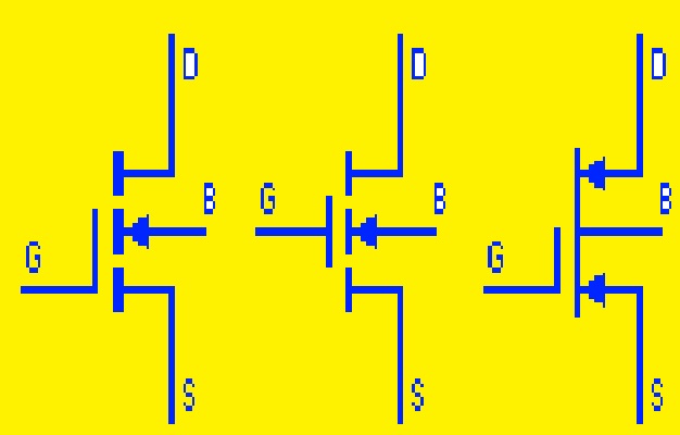
Enhancement Type MOSFET with Bulk
This type of enhancement MOSFET comes with 4 terminals. The extra terminal is called the Bulk or body terminal. it is not an input nor output pin but is used for grounding purposes. It is used internally connected with source pin that is released in symbol to show a schematic with less clunky wiring.
Logic Level FET Transistor
Logic-level FET transistors are made to be used with digital logic systems. They are used for switching heavy loads when provided with digital logic. Positive logic voltage normally is five volts and the gate source starts conduction at the highest current.
Operating Conditions of Transistor Symbols
FR
- In this condition, the emitter-base junction is forward-bias, and the collector-base junction is connected in a reverse-biased state. Transistors in the active region and collector current based on emitter urrent. Transistors that operate in this region are part of amplifier circuits.
FF
- For this state, both junctions are forward-biased. The transistor is saturated, and the collector’s current is independent of the base current. Transistors work like closed switches.
RR
- In this condition both currents are biased. The emitter does not supply the majority of carriers to the base, and carrier current is not collected through collectors. So transistors work as closed switches.
RF
- The emitter-base junction is reverse-biased, and the collector-base junction is forward-biased. The collector is less doped than the emitter junctions and does not provide majority carriers to the base.
Transistor operating conditions
Here are the maximum rating and biasing conditions for the 2N2222A are shown.
| Parameter | Maximum Rating | Biasing Condition |
| Collector-emitter voltage | 40 volts | 12 Volts |
| Collector current | 800 milliamperes | 100 milliamperes |
| Emitter-base voltage | 7 Volts | 0.7 Volts |
| Base current | 20 milliamperes | 5 milliamperes |
| Power dissipation | 625 mW | 200 milliwatts |
Advantages of transistors
- It helps with the easy testing with a multimeter.
- It is used for regulating power supply to electrical loads in choppers and inverters.
- It has features of operating at a switching frequency of about 10 to 15 KHz.
- Its compact size helps to connect many transistors on board.
- It is used as a switch due to switching frequencies.
- Its low working voltage helps it be safe and is best for tight spaces.
Disadvantages of transistors
- Transistors produce heat during working, and this heat must be dissipated to avoid damage to the device. It required heat sinks or cooling fans.
- Transistors can handle the limited voltage. high value than this limit can result in damage to the device. So transistors are not good to use for high-power uses.
- Transistors come with non-linear responses to input signals that can cause distortion in amplifiers. This distortion can be reduced with the use of feedback circuits, but it makes complex circuits.
Applications of Transistors
- The main uses of transistors are switching and amplifier circuits.
- Transistors produce current flow based on light colliding with them, called phototransistors.
- BJT can result in a high current flow from the emitter to the collector when a small current flows through the base.
- FETs work as voltage-controlled devices. FET comes with high input impedance and helps to run small currents through them.
- Heterojunction Bipolar transistors can offer high-speed switching speeds and are used in analog and digital microwave applications. It is easy to make and offers good lithographic products. It is used in mobile and laser driver amplifiers.
Read Also:
- Difference between Vacuum Tube and Transistor
- Introduction to C945 Transistor
- Introduction to 2N2219 NPN Transistor
- 2N3702 Transistor Working & Application
- Introducing to BC556 Transistor: How It Works And Where You Can Use It
- What is PNP Transistor: How It Works and Its Applications
- Difference Between NPN vs PNP Transistor
Faqs
What are the transistor symbols?
| Name | Description |
| Darlington Transistor | Made from 2 bipolar transistors. Has total gain of the product of each gain. |
| JFET-N Transistor | N-channel field-effect transistor |
| JFET-P Transistor | P-channel field-effect transistor |
| NMOS Transistor | N-channel MOSFET transistor |
What are 3 types of transistors?
- The transistor is divided into three types that are bipolar transistors (bipolar junction transistors: BJTs), field-effect transistors (FETs), and insulated-gate bipolar transistors (IGBTs).
What are PNP and NPN transistors?
- Bipolar junction transistors have two subtypes: NPN and PNP transistors. NPN transistors come with two N-type semiconductor materials separated through a thin layer of P-type. PNP transistors come with two P-type semiconductor materials separated through a thin layer of n-type.
- The transistor is a combination of transfer and resistance. Since it transfers the resistance from one end of the device to another end. So it is called a transistor. It has high input resistance and low output resistance.
- Two main transistor types are BJT and FET.
- The transistors work as switches or gates for electronic signals, opening and closing electronic gates many times in a second. It makes sure the circuit is on if the current is passing and switches off if it is not. Transistors are used in complicated switching circuits that come with modern telecommunications systems.
- PNP switches on through a low signal while NPN switches on through a high signal. In PNP transistors, P denotes the polarity of the emitter terminal and N denotes the polarity of the base terminal.
- In NPN, N denotes the negatively charged coating of material, and P is the positively charged layer.
- The MOSFET is commonly used. Its main use is to control conductivity, or how much current flows, between source and drain terminals based on the voltage provided to gate terminals.