 The Common Source JFET (junction field-effect transistor) Amplifier circuits usages JFET as their chief energetic component for delivering higher input impedance appearances. Mostly signal amplifier circuits are made by bipolar junction transistors like common-emitter transistors, but where a small signal has to amplify where FET is used as an amplifier.
Input impedance in this category of the transistor is better than BJT and offers less value of distortion for the output generated signal.
Introduction to Common Source JFET Amplifier
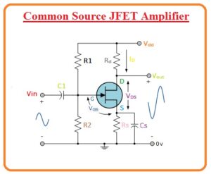
- The design of this amplifier’s circuit depends on a JFET. To create this amplifier first of all you should search a proper Q- point for exact biasing of the JFET amplifier with a single arrangement of Common-source (CS).
- For this interpretation look at the circuit diagram, in this circuit, we are using N channel JFET, which is connected in a common source arrangement.
- The voltage at gate of JFET is supplied by a potential divider system which is created by a resistance R1 and Resistance R2 and it (gate) is biased to work in its saturation region. That is equal to the energetic(active) region of BJT.
- The JFET receipts practically no current at gain letting the gate to be work like an open circuit.
Comparison between JFET and BJT
| JFET | BJT |
| It has Gate ( G ) in place of gate | It has Base ( B ) in place of Gate |
| It has Drain ( D ) instead of collector | It has a Collector ( C ) instead of a drain |
| It has a Source ( S ) terminal | It has Emitter, ( E ) terminla |
| It has Gate Supply ( VG ) | It has Base Supply, ( VB ) |
| It has Drain Supply, ( VDD ) | It has a Collector Supply, ( VCC ) |
| Ita has Drain Current, ( ID ) | It has Collector Current, ( IC ) instead of drain current |
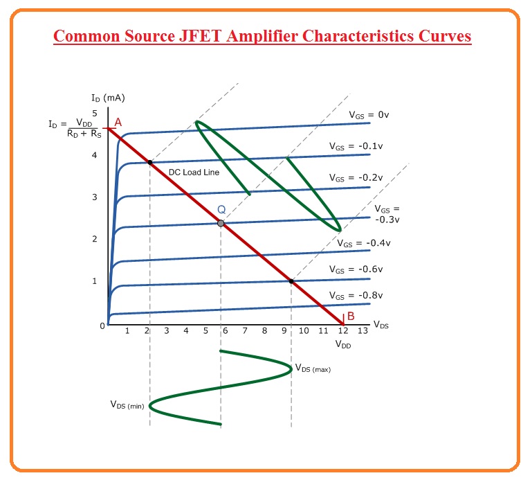
Characteristics Curves of Common Source JFET Amplifier
- We can see that location of point Q is usually located at the middle of the line of a load.
- It can be measure by the mean of gain voltage (Vg) which is biased negative way because the junction FET is a reduction style expedient.
- As we discussed in the last article, the output of a common emitter amplifier is 180 degrees out of phase from its input. In the case of a common source JFET, the results are the same.
- One of the chief drawbacks of Reduction mode junction FET is that they should be reverse bias.
- If, for some reason, this biasing fails, then the gate-source voltage can rise, which causes an increase in drain current subsequent to the letdown of the Vd.
- the higher channel resistor, Rds of the JFET, which is joined with higher inactive stable Id cause the device to become heat up so an extra heat absorber is required for its proper working.
- Though, the maximum of the difficulties related with the use of JFET can be significantly abridged by means of MOSFET.
JFET (junction field-effect transistor) Amplifier Current and Power Gains Parameters
- The value of gain current (Ig)of a common source junction FET amplifier circuit is very minor since of the enormously higher gate impedance, Rg.
- Therefore this amplifier has a very decent proportion amid its input and output impedances and for any quantity of IOUT it will have a higher gain.
- Due of this reason these amplifiers are very appreciated as impedance corresponding circuitries work as a voltage amplifier.
- Working of Common source JFET Amplifier
- In the given diagram there is a circuit of the common source amplifier circuit, in this circuit, we are using N channel JFET.
- We can see in the circuit that the capacitor C1 and capacitor C3 are working as input and output coupling capacitors.
- Resistor (R1) in this circuit is the gain resistance. .It stops undesirable charge stores on the gate by given a discharging track for a capacitor (C1).
- Resistance R2 and capacitor C2 deliver source self-biasing for junction FET. Resistance R3 is a load resistance of drain which works like collector load resistance.
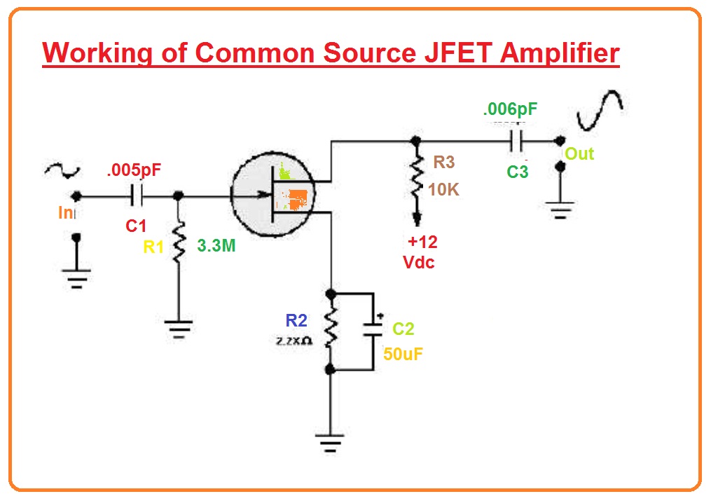
- From the picture, we can see that there is a 180-degree phase between input and output like a common emitter amplifier circuit.
- The cause for this 180-degree change can be understood by the working of N channel JFET.
- at the positive fluctuation of the input signal, the quantity of reverse biasing on the (P) gate substance or material is abridged, thus growing the active cross-sectional part of the channel and lessening the resistance between source and drain.
- When resistance cuts, current moving in the JFET upsurges. This upsurge causes the voltage loss across resistance (R3) to upsurge, and due to this reason drain voltage decreases.
- . at the negative change of the rotation, the quantity of reverse biasing on the gate of the junction FET is amplified and the act of the circuitry is inverted.
- This causes the output signal to be 180 degrees out of phase.
FAQS
What is a common source JFET amplifier?
- The amplifier circuit comes with N channel JFET but it is also equivalent to N channel depletion mode MOSFET since has a circuit similar to that is changed in FET configured in the common source circuit.
What is the most commonly used FET amplifier?
- The common type of FET amplifier is the MOSFET amplifier employs a metallic oxide semiconductor. The main features of FET to use as amplifiers since has high input impedance and low output impedance.
What is the main advantage of a JFET amplifier?
- JFET input amplifiers provide different advantages for high-speed circuits since has high Z input, good distortion features and high-speed settling.
What are the advantages of a common source FET amplifier?
- The main features of a common source amplifier is high voltage gain, good input impedance, and good output impedance. Common source amplifiers and common gate amplifiers are 2 main types of amplifiers used for analog circuit design.
Read also