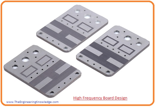
 The high frequency is the type of PCB (Printed Circuit Board) like other categories. It operates at a frequency range from five hundred Mega-Hertz to two Giga-Hertz it is also compatible with microwaves, and radio frequency signals. Due to its capability to transmit signals longer distances it is used in radar, industries, and military applications, as well as in medical devices.
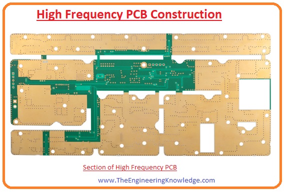
In the previous tutorial, we discussed detailed its introduction, features, and applications. In today’s post, we will have a look at its construction and design with detail. So let’s get started with High Frequency PCB Construction.
High-Frequency PCB Construction
- The construction of this board is time taking and costly process so we should follow some serious factors about its construction.
- These parameters depend on the quantity that you are going to create, your budget, your design layout, and some standards that are commonly used in the world for construction.
- After setting these factors, you can start to design a high-frequency board.
- for construction, you should also follow these steps.
- The first thing is to monitor the frequency of the PCB board.
- Mostly higher frequency printed circuit board uses fifty-hertz frequencies for the better performance ofthe circuitry that is used.
- You can check the dimensions of traces on the PCB board, whether you are working on a high-frequency board or not.
- If your find trace is over the 3rd the rise time of your device switching speed, then your operation board is a High Printed Circuit Board.
- After that find that either your board is a single unit or has different partitions.
- If there are multiple divisions on your board then it is a High-frequency board.
High-Frequency PCB Manufacturing Processes
PCB Design
The HF PCB board manufacturing started with the design of quality features, and according to project demand. Perform all testing methods for proper manufacturing.
Etching
- The design is printed on internal copper layers and copper layers configured with base materials of the board that show the layout of the board. After printing and engraving on copper, the internal and external layers are accurately configured and aligned.
Electroplating
- In this step, plating of inner and external copper layers is made and installed after every layer is made separately.
Holes Drilling
- When layers are made, drilling is done with the use of drilling machines like X-ray machines that make holes at defined positions.
Board Cleaning
- After the etching process, the board is clean and has had extra copper. Now the board is ready for painting with the use of chemicals that are used for PCB painting and connecting layers.
Solder Mask
- In this step, solder mask is applied on the board for solder mask preserving copper, and all layers of board’s silk finishing are done.
Test
- • The HF PCB board now passes through different testing methods like insulation tests, electrical performance tests, and some other tests done to make sure that the board is ready to use for practical work.
High-frequency circuit boards
- Due to the increase in the complexity of electronic elements and switching circuits, high-speed signal movement and high-speed transmission of frequency are needed.
- Because of the small pulse rise time in electronic devices, high-frequency techniques must observe the conductor dimensions in electronic elements.
- According to different factors, high-frequency signals are reflected at the circuitry boards, in other words, there is a change in impedance according to the transmission component.
- To avoid this fact there should be certain features and implementation at a high level of process control
- The main causes for impedance in HF PCB are generally the conductor-traced structure, creation of layers, and dielectric constant.
HF PCB by PCBWAY
- Now i hope you have become well aware of HF PCB board. nowhere i main things i want to mention that from where you can get services related to the HF PCB.
- Numerous manufacturers is working in the market but each has its features but The most reliable and trustworthy manufacturer of HF PCB is PCBWAY.
- It is a China-based PCB online manufacturer that offers PCB-related services on reasonable prices and within a given time interval.
- It has a high experienced team of technicians and engineers for the creation and design of PCB according to tour desired requirements.
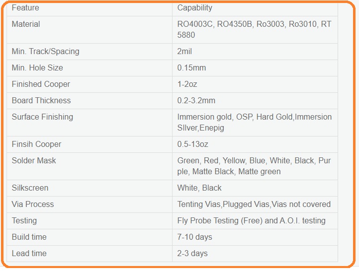
- The materials used of HF PCB at PCBWAY are RO4003C, RO4350B, Ro3003, Ro3010, and RT5880.
- The least size of spacing is two mils.
- The least hole size for the HF PCB is 0.15 millimeters.
- The board thickness is available in 0.2 to 3.2 millimeters.
- The main features and capabilities offered by the PCBWAY for the HF PCB board are mentioned herein below figure with the details.
HF PCB Designs
- Multiple circuit boards are supporting instantly in the designing of boards. There is a need to search for accurate substrate, conductor dimensions, and impedance values.
- The generally preferred material for the substrate is PRFE having less loss.
- With that multiple layers are used for controlling impedance.
- The range of micro vias is up to seventy-five micrometers.
Materials for HF PCB
- High-frequency boards are used for such applications where wireless applications employ different data rates in the upper gigahertz having certain requirements for the material.
- The features for material used are adapted values of permittivity.
- Less attenuation for effective signal transmission.
- Homogeneity in creation has less value fo tolerances in insulation thickness dielectric constant.
- In different applications, there is enough to use FR4 with the combination of accurate layer creation. With that, the procedure helps to improve through the use of well accurate dielectric material.
- Such features are offered through less loss factor, less dielectric constant and do not depend on the varied value of temperature and frequency.
Applications of HF PCB
- The main applications of HF PCB are mentioned here with detail.
- It is used in the creation of different types of instruments used in military purposes.
- It is used in medical devices for the creation of different tools.
- It is used in industries for different machines and equipment where hf frequency is employed.
- The devices created through HF PCB are used in radar applications for communications.
Advantages of High-Frequency PCBs
Heat Resistance:
- HF PCB board has high resistance to heat since it comes with materials that easily distribute heat.
High Transfer Speed:
- This feature makes it useful for high-level advanced device circuits.
Signal Management:
- It has control for signal management and reliable transmission with low losses.
Durability:
- These boards are durable nature and help to provide ga ood working life for circuits with high efficiency.
Low Cost:
- It is small size and reduces cost with use of low-cost wires.
Read also
- Comprehensive Guide to PCB Voltage Regulators: Types and Applications
- PWB vs PCB: Differences and Similarities
- What is Rogers Ceramic PCB and How Much Do Those PCBs Cost
- PTFE PCBs: The Ultimate Solution for High-Frequency Applications
That is a detailed post about HF PCB I tried my level best to explain about this board. If you have any further query, ask in the comments. Thanks for reading, have a nice day. See you in the next post


