 Hello, readers welcome to the new post. Today we will discuss Introduction to 741 OP-AMP. The operational amplifier 741 also known as LM741 is a commonly used operational amplifier IC that is used to solve mathematical editions and as an amplifier. It is used to solve mathematical operations like addition, subtraction division differentiation, and some other operations.
It has a high value of gain and is designed through the use of BJT or FET which can get power through positive and negative sources. Firstly it was created by Fairchild Semiconductor in 1963. In this post, we will discuss its working, features, and some other parameters. So let’s get started Introduction to 741 OP-AMP
Introduction to 741 OP-AMP
- LM741 is a general-purpose operational amplifier that is DC coupled high-gain voltage amplifier.
- Its design comes with one operational amplifier. It operates like a comparator as have an operational amplifier circuit that provides a comparison between two signals which are inverting and non-inverting signals.
- It is used for solving different mathematical equations. With that has a high gain so used for voltage amplifier circuits. It operated with one or two power supply circuits
- It is a monotheistic IC and configured to operational amplifiers.
- 741 number shows that operational amplifiers have 7 inputs, that are 4 inputs and one output pin.
- It comes with high voltage gain so used for integrator, summing amplifier and also for general feedback circuits
- It also comes with short circuit protection circuits and inner frequency compensation circuits
- It has three packaging
- 8 Pin SOIC
- 8 Pin DIP Package
- TO5-8 Metal can package

741 OP-AMP Features
- The main features of 741 operational amplifiers are discussed here
- There is a single operational amplifier designed with 741 op-amp
- It has inbuilt short circuit and overload protection circuits
- Its common packaging is TO-99, CDIP & PDIP
- It uses less power during operation
- It has less value of CMRR
- It does not need any outer frequency compensator
- It saves from latch-up if the common mode value is high
- Its less general and highest power values are ±10v, ±15v, and ±22v respectively.
- The working temperature for this device is -50 to 125 ˚C.
- Its input current is – 1.7 to 2.8 mA.
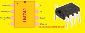
741 OP-AMP Pinout
- Its eight pinouts are discussed here
- Pin 1, and 5 are offset null pins that remove the offset volts and balance input volts
- Pin 2: in inverting terminal pin
- Pin 3 is the non-inverting input pin
- pin 4 is a negative supply pin as well used for ground connection
- Pin 7: is a positive voltage pin
- PIn 8: is not used for any connection

741 OP-AMP Circuit Manufacturing through PCBWay-OEM Service
- PCBWAY is a China-based PCB supplier that provides PCB-based services to its customers. With that offered electronic projects-based services. They also introduced different services for their clines at great prices and quality.
- Some months ago PCBWAY also introduced OEM service for their clients. That is one stop electronic manufacturing service, through using these features you can transform your idea into real products. Like the design of your 741 operational amplifiers can be converted into practical devices.
- PCBWAY-OEM helps their clients through customized solutions, pass production, and other related services like design, component procurement for projects, PCB manufacturing, patching, and plug-in testing assembly at one platform https://www.pcbway.com/oem.html

OEM Service Processes
Quotation
- To get a quote for OEM service you have to submit a request for Quote RFQ online that has two portions. The first one is basic business information, having details of the company, address, industry, etc and the other is project info, like project category, project name, outsourced processes like your project, etc. All these details help the PCBWAY team to evaluate the project with detail and effectively with if you have any samples related to the project can share them as a reference. There is NDA file will be signed before this process
Project Review
- When you submit RFQ, they proceed to the project review stage. Their engineers set up to assess the product manufacturability, reliability, and other related features and with that, they will make a rough measurement of the budget for equipment. If they think that they have sources to make the project then a formal project order will be made
Confirm Detailed Requirements and Reach an Agreement
- They will contact you to make sure of some details of the project and your final prices. With that, they also offer approximate price quotations for you based on the supply of different components. If you select that prices are in your range and cooperation intention can be reached then they sign a formal cooperation agreement. With that, they will then give a final cost list and deliver a schedule based on raw materials inputs components, labor inputs, and other sources
Samples & Mass Production
- After completion of all the processes explain earlier their factory arranges the production for samples like mold review, desing, component confirmation, and many other processes. If there are any issues exist during the sampling process, they will inform you on time to ensure that you get feedback on every stage of production seamlessly. They will then provide completed samples to you for confirmation when completed. When samples are according to your need for operations and free from any faults masse production will be done
Delivery& Payment
- The finished product will be sampled and tested before delivery. If there is no issue exist with the test results delivery and payment will proceed.
- Here the general process of OEM service is explained. Further details can get here.
Introduction to OEM
- The video tutorial also has shown here.
- In the final must-visit PCBWAY OEM service to convert your ideas of projects in reality in good prices with quality.
- PCBWAY currently has introduced its Christmas Sale where you can get huge discounts to your projects and some other PCB-related products. So If you have to create your LM741 project or any other electronic project must visit PCBWAY Christmas discounts
2022 PCBWAY CHRISTMAS BIG SALE
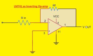
LM741 as Inverting Op-amp
- If the input supply is attached to inverting PIN 2 of the amplifier and feedback with output pin number six then the operational amplifier circuit will be inverting.
- The value of gain will be
- GAIN=Rf/Ri
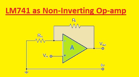
LM741 as Non-Inverting Op-amp
- If the input supply is attached to non-inverting pin number 3 and PIN 2 is used as feedback to output PIN6 then the operational amplifier is non-inverting configuration.
- Gain value can be found using this formula
- GAIN = 1+ (Rf/R1)
Internal Schematics Op-Amp IC 741
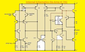 The structure of 741 IC is created through the use of twenty transistors and 11 resistors. All these components are configured in a single casing. The connection of these components can be seen here
- In this circuit inverting and noninverting points are attached to transistors Q1 and Q2. Both these transistors are NPN transistors.
- The output of these transistors is attached to transistors Q3 and Q4. This structure separated both inputs to transistors Q3 and Q4 and avoid feedback to occur
- The voltage variation at the input terminal of the operational amplifier causes current to flow in the inner circuitry and also affects the functional range of the transistor in the circuitry
- To avoid this configuration 2 mirrors were used. Transistor Q8 and Q9 and Q12, Q13 pairs are attached in structure to make two mirrors circuits
- Transistors Q8 and Q12 are working as regulating transistors that set voltage levels at the emitter-base junctions for related transistor pairs. This voltage value can be regulated correctly to a certain decimal of mv to permit the needed current to flow
- The first mirror is created by Q8 and Q9 is made to input circuitry 2nd mirror circuitry is created through Q12 and Q13 is attached to output circuitry. Third mirror circuitry created through Q10 and Q11 functions as high impedance connection among input and negative sources.
- The transistor Q16 with resistors 4.5-kilo ohm and 7.5-kilo ohm makes voltage level shifter circuitry that reduces voltage level from the amplifier at the input part through Vin before it passed to other circuitry. It is made to avoid signal distortion at the output amplifier part of the structure
- Transisor Q15, Q19 and Q22 are created to make Class A amplifier and transistors Q14, Q17 and and Q20 make output stage of operational amplifier 741
- To make a balance for any irregular at the input phase of differential circuitry transistors Q5, Q6 and Q7 are configured to offset null +Ve and -Ve and balance both inverting and non-inverting input.
Op-Amp IC 741 Applications
- It used as general feedback circuits
- Used in active filter circuits
- It is part of multivibrators
- It used as a summing amplifier
- Used as integrator or differentiators
- Used in DC amplifiers
- it is part of the comparator
That’s all about 741 OP-AMP all related parameters has to explain if you have any questions ask them below thanks for reading.


