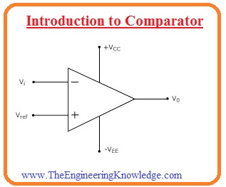
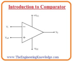
 Hi, readers welcome to new engineering-related posts. In today’s tutorial, we will have a detailed look at Introduction to Comparator. The comparator is such electronic circuitry that uses to find the comparison among 2 different values of current and voltage. The output of this circuitry tells about the value which is greater.
There are 2 inputs terminal of this device where analog values are given and one output terminal which shows te resultant output in digits. The circuitry of this module comprises of the differential amplifier which provides a large value of gain. The common application of these instruments is ADC and relaxation oscillators where it finds the values and transforms them in the digital form. In today’s post, we will have a detailed look at its working, operation circuit, and different parameters. So let’s get started with Introduction to Comparator.
Introduction to Comparator
- The comparator is a type of operational amplifier that gets 2 inputs and find their comparison and indicates there relationship in the form of larger or lesser.
- These circuits are used in such applications where high switching speed is required and with numerous features it has like inner reference voltage and high-speed propagation delay.
- Some category of comparators such as ultra-speed comparators has a value of propagation delay of five hundred picoseconds.
- Since the output shown by the comparator is exists in a single state so these modules are used to provides interlinking between analog and digital circuitry.
- In some applications where operational amplifiers are operating in open-loop are used as comparators.
- These amplifiers have some drawbacks like less operation speed but due to high gain they has the ability to find small value difference between input terminals
- In simple words the comparators does not perform the function of operational amplifier but operational amplifiers can also work as comparators.
Op-Amp as Zero-Level Detector
- The common uses of an operational amplifier in the form of a comparator is to find the value of input voltage larger than the specified range.
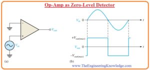
- In the below figure you can see the circuit of zero level detector.
- You can see that the inverting terminal at the input is attached with the ground for the creation of 0 level and input wave is given to the noninverting terminal.
- Due to the large value of open-loop gain, the less value of voltage among 3 inputs terminals causes the amplifier to move to the saturation condition that reason the voltage to move to the required value.
- Let us assume that the value of the open-loop gain of the amplifier is one lac.
- If the value of the voltage difference between 2 terminals is 0.25 millivolts so the output voltage will be twenty volts.
- The figure denoted as b’ indicates the output-input sine signal given at the noninverting terminal of 0 level detector.
- When the signal at input is positive the output will also highest positive value and when the signal at input moves from a positive maximum to the negative maximum the resultant output will be the highest negative.
- In figure you can see that output is a square wave so in such applications where the square signal is used zero level detector is used.
What is Nonzero-level Detectors
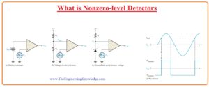
- The 0 level detector discussed above can be used non zero level detector with some modifications and it fins the value of positive and negative voltages if the certain value of reference voltage source is linked with the inverting input in the below figure you can see it.
- The detailed circuit is shown in figure denoted as b’ where reference voltage denoted as VREF gives values of.
VREF =R2/(R1 + R2)(+V)
- In this equation the (+V) indicates the positive operational amplifier dc power supply.
- The circuit denoted as c’ comprises of Zener diode for setting the value of reference voltage which is equal to the Vz.
- Till the value of Vin is low than the reference voltage then output will has highest negative value.
- When the value of input voltage is larger than the reference voltage then output will be at highest positive level it shown in figure denoted as d’.
What is Effects of Input Noise on Comparator Working
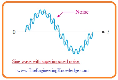
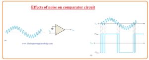
- In some applications, there is undesired variation in voltage value is occurs at the input side. The noise or undesired voltage variation interlinked with the input voltage as you can see in below figure. It shows the sine waveform.
- For understanding the practical results of nouse voltage let suppose that since waveform with less value frequency is given to the positive terminal of an operational amplifier that is operating as comparator shown in below figure denoted as a’.
- The figure denoted as b’ indicates the sine waveform with noise signal and output signal.
- When the value of sinusoidal waveform goes to the zero the variation caused by the noise signal can cause the net input fluctuate over zero value certain times and it causes the faulty output.
Reduction of Noise Effects through Hysteresis
- Due to noise signal at input faulty output is created since comparator changes state from negative output to the positive output state at similar input voltage value which changes the condition in the reverse state from positive to negative.
- When the value of input voltage is about the reference voltage unstable state exists and less noise variation causes the comparator to change its state from first to second.
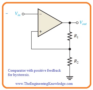
- To decrease the response of comparator towards the noise the method incorporating positive feedback which known as hysteresis is used.
- Hysteresis indicates that the large value reference when the input voltage moves from less to high value than it moves from high to low value.
- The 2 reference points are denoted as UTP or upper trigger point and LTP or lower trigger point. This 2 hysteresis is created with the use of positive feedback configuration.
- Note that noninverting input is attached with the voltage divider circuit created with resistance which is part of the output voltage is going back to the input.
- In this condition, the input signal is given at the negative terminal of input.
- In the below figure the function of a comparator with the hysteresis is explained.
- Let us suppose that the output voltage has an extreme positive value. The voltage giving back to the noninverting input is VUTP and define as,
VUTP=R2/(R1+R2)(+Vout(max))
- If the value of VUTP is less then the input voltage the output voltage becomes negative extreme shown in figure denoted as a’.
- In this case, the voltage giving back to the noninverting input is VLTP and denoted as.
VLTP=R2/(R1+R2)(-Vout(max))
- The input voltage should be less than VLTP it can be seen in figure denoted as b’ before this point comparator will change state from highest negative voltage level to the highest positive voltage.
- It indicates that less quantity of noise voltage provides no influence at the output it is shown in figure denoted as c’.
- The comparator created with the hysteresis is called a Schmitt trigger.
VHYS= VUTP – VLTP
That is a detailed post about Comparator if you have any further query ask in comments, Thanks for reading. Have a good day.
