 Hello, readers, welcome to the new post. In this post, we will learn how to reduce the PCB Board Size for Projects. PCB is the very element of each and every device and project simulated in electrical and electronic engineering projects. There are different types of boards used in the creation of your projects and designs, like single-sided PCB, double-layer PCB, multiple-layer PCB, and aluminum PCB etc. Every board offered its different features and parameters to make the device. But the main fact is how we use these boards to create our project effectively and reasonably, and with a minimized size for our projects. It is a very certain and sometimes very difficult way to do this process since it needs certain skills and different tools that a new person does not have and can afford to do so.
Here i want to mention that if you are new to the PCB world and do not know how to customize the board properly for your projects. I will make this process easy for you by introducing a PCB designer and manufacturer that can come with all the skills and tools that are not available to the common person. That is PCBWAY. It is a China-based PCB manufacturer that provides different services related to PCB boards and the manufacturing of PCB boards. They are facilitating all over the world related to PCB board manufacturing and different engineering projects. So if you are facing difficulty in reducing the board size that you are going to use in your projects. Must visit them, they are equipped with all types of tools used for the PCB assembly and design, and drawing to the dimensions of your board.
Their well-skilled and well-equipped engineering team will guide you on how you have to sort out your problems related to the board and customize the board. They will also help you to properly design your board from the base to the completion of your projects. You just have to send the different parameters related to your projects after that,t they will handle all tasks and operations related to your board. Here I also share some tips that will help you make your board effective. So let’s get started with how to reduce the PCB Board Size for Projects
How to Reduce the PCB Board Size for Projects
Usage of Multiple-Sided PCB Board
- The use of multiple layers can make your board simple and easy to configure for components that are used for projects.
- As multiple-layer give larger room and space for component assembly than single-layer boards.
- Over the multiple-layer board, different layers exist to make the design connection properly.
- The creation of multiple layers is somewhat difficult, but its larger space for connection makes the simulation of the project simple and complete on one board.

Usage of Smaller Structure Components for Projects
- In hte market there are diffent compoents of difent ratins exist. So engineers try to use larger size elements that are easy to handle for them.
- So in place of usage of this component that has a larger size try to use a component that has a smaller size but has the same value of rating value that comes from the larger size devices.
- The use of small-sized elements will help to make our circuit easy, simple, and reasonable size.
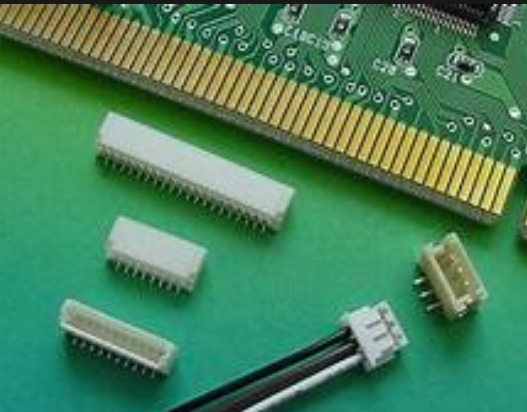
Connector Size Should be Small
- With the use of small-sized project components, there should be a usage of small-sized components that generally take up less space on board.
- SO must try to use and select a connector that is in small size and has a reasonable configuration that can handle our board.
Reduce the Footprint Size
- Generally, the size of footprints used for elements of projects is larger than our requirements which results in an increment in the bard size.
- So, before selecting the size of the footprint of any device, read the datasheet and then design the dimensions of the footprint of the elements and make changes in the design according to board arrangements and project requirements so our board remains in control.
Usage of High Copper
- In some projects, there is the usage of a larger value of current for different devices and components that can cause heat in the projects and result in damage of our projects.
- To minimize the effect of heat, different components are used at the board, like a heat observer that makes our board larger and the size increases.
- In place of the usage of a heat absorber, we should use traces of high-value cooper that will help to reduce the heat in the circuitry and help to make the board size reasonable.
Control Board Physical Dimensions
- When you are designing the board, try to maintain the length and width at a certain level that can handle all components reasonably used in the project.
- Try to use such elements that can be accurately employed at the board in a certain dimension of the board.
- So here I want to more that if you are new to PCB and have less knowledge about PCB designing and different parameters, you visit PCBWAY. It can help you to customize your board accurately and reasonably can making your projects very good and well-working for you.
That is all about the How to reduce the PCB Board Size for Projects if you have any further query ask in the comments. Thanks for reading have a nice day.


