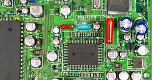
 Hello, readers welcome to the new tutorial. In this post, we will learn How to Free Assembly for Your PCB. PCB is a printed circuit board that is employed in different projects in different manufacturing processes and designs. PCB is a chip where small layers of coppers are assembled. It is created with the fiberglass coppers traces and some other components of metals.
When any project or configuration of different components is positioned on the board called PCB assembly or PCBA. The assembly of the PCB board is simple and different steps are used for this purpose. In this tutorial, we will learn different parameters related to PCBA and learn how to get a free PCB assembly service. So let get started.
What is PCB Assembly
- If different components like a capacitor, diode, inductors transformer, etc are assembled on the PCB board for the creation of any device or project called PCBA.
- There are different manual and automatic instruments used for the creation of PCB assembly.
- The PCB assembly is not like the manufacturing process of PCB. For manufacturing, PCB different steps are done such as the design creation of PCB and PCB prototype.
- After PCB creation there is different components of electronic are placed on the board. Placing of different components on the board relies on the category of PCB, the objective of PCB board, and electronic components.
Components Required for PCBA
- Different components needed for PCBA are listed here
- PCB board
- Electronic components such as diode, capacitor, transformer, etc
- Soldering components such as solder paste, solder wire solder bar, solder balls
- Soldering flux
- Testing machines
Process of PCB Assembly
Some steps for PCB assembly are described here with detailed
Solder Paste Stenciling
- In the first step, there is solder paste is placed on the PCB board. It is like silkscreen printing. Only where the paste is applied their components have placed.
- Solder paste is a gray color material that has small size metallic components of ball-shaped called solder. Their composition is 0.5 percent copper three percent silver and 96.5percent tin
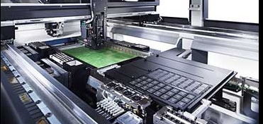
Pick and Place
- Now move the board having solder paste to the pick and place machines, robotic instrument SMD at the created board.
- SMD is considered for non-connector elements at the PCB board.
- It was a manual procedure done through the use of tweezers through which components were placed with hands.
- Currently, it is done through an automated process. So errors that occur by humans can be decreased through this process
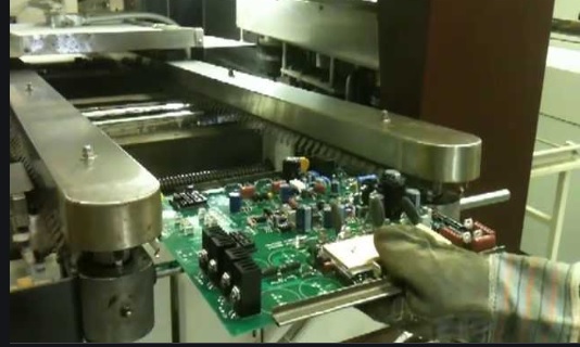
Reflow Soldering
- After placing the solder paste and surface mount elements must fix at their respective places. It shows that solder paste needed to become solid. This process is called solder paste.
- PCB is shifted to a conveyor belt that passes through the reflow oven. There are heaters exist in the oven having a temperature of about two-fifty centigrade
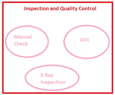
Inspection and Quality Control
- After the reflow oven process, there are some tests performed to check the quality of the board. During heating reflow affect the position of come connection and some short circuits occurs that disturb the position of components.
- There are finding and detection of faults can be done through the different processes listed here
- Manual
- Automatic Optical Inspection
- X-Ray inspection
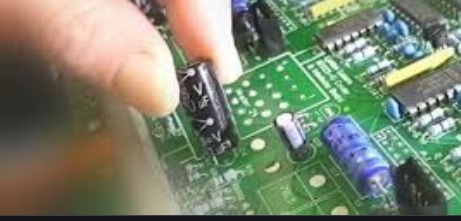
Through-Hole Component Placement
- According to the category of PCB board over which PCB assembly is done, the board can have different components than normal SMD. Those are plated through-hole components.
- A plated through-hole is made on the board and used by the PCB elements to use these holes for the movement of signal from one part to another.
- Through-hole component placement used manual soldering and wave soldering for component placement than solder paste assembly.
Final Testing
- when soldering of PCBA is completed final testing of the board is done. This testing step is called a functional test.
- This test checks the normal working of board by providing normal conditions working.
- The power supply is linked and finds the PCB electrical operating features are measured through testers monitors.
- SO different aspect related to volts, current are measured and final products is completed after the success of the test.
Free Assembly for Your PCB
- Till now you have get a detailed overview of PCB assembly with details and will tell you how you can get the free PCBA service for your PCB board. There are many PCB manufacture working but not like the JLCPCB that is very well known and most trustable and reliable PCB providers also offering the chance to get free PCB assembly.
- You can get your PCB manufacturing in just two dollars and have them assembled from $0.
- For one to four Layer PCBs with 1oz. Cu, HASL surface finish, you can get below special offers.
| Layer | PCB Size | Qty | Price |
| 1-2 Layer | 100x100mm | 5 pcs | $2 |
| 4 Layer | 100x100mm | 5 pcs | $2 |
- Get Instant Quote Online at https://cart.jlcpcb.com/quote
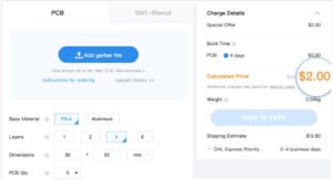
Free PCB Assembly for PCB orders
- Each customer of JLCPCB can avail $24 Coupon for SMT assembly on monthly basis. If you place any order will get 3 coupons ($9 + $9 +$6) at the beginning of the afterward month. The SMT coupons can be found in your Account > Coupon section.
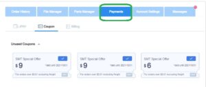
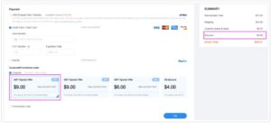
- When you checkout, just choose a $9 SMT coupon, and the discount will be automatically applied during checkout. Which can cover the $7 setup fee, $1.5 stencil fee, that’s to say, the SMT assembly starts at $0
That is all about the How to get Free Assembly for Your PCB. I have all detailed about the PCB assembly and parameters. If you have any further query ask in the comments. Thanks for reading have a nice day.

