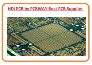
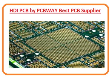
 Hello, friends welcome to our site for a new interesting post. In this post, we will have a detailed look at HDI PCB by PCBWAY Best PCB Supplier. PCB stands for a printed circuit board that is a very commonly used circuit board in the electronic industries and engineering projects. Almost every electronic device either it is your calculator or laptop over which you are reading this post comprises of PCB.
There are numerous categories of PCB single layer PCB, double layer PCB, multilayer PCB rigid PCB, etc. To get these PCBs there are numerous PCB creators are working in this world but there is one and only PCB supplier which I always suggest is PCBWAY. I am also a user of this PCB supplier that provides the best and high-quality products and its products have good quality at a reasonable price. In this post, I will explain about their product which is HDI I hope you will select PCBWAY after reading this post. So let’s get started with HDI PCB by PCBWAY Best PCB Supplier.
Introduction to HDI PCB
- The HDI stands for high-density interconnects PCB is a modern form of PCB that has introduced a new product in the PCB industry.
- This board provides larger space than the other boards so there is small size vias and pads that can be created.
- At this board blin and buried are assembled time size vias are also assembled that have a size range of 0.006 or sometimes less than it.
- The use of HDI techniques in electronic engineering provides facility tho the engineers assembled more components at both surfaces of general PCB in some certain requirements.
- The development of via in pad and blind via techniques facilitates the engineers to assemble small-size elements at a small distance.
- That provides high-speed signal transmission and also reduces the loss of signal.
- The common application of HDI PCB is in mobile phones, such devices that have touch display computer laptops, digital cameras.
Vias Used in HDI PCB
- There are 3 types of Vias used in HID PCB for the optimization of spaces required for interlinking among layers and different elements of circuits.
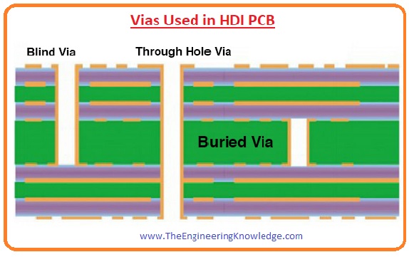
Microvias
- These vias have a very small size and can be created with the use of lasers. Their dia is very less than normal vias. Micro vias have 2 further types. Stacked and Staggered.
Blind Vias
- These vias are used for the interlinking of the exterior layer to the internal layers and have access to a single outer layer.
Buried via
- It can interlink the internal layers to a similar substrate or numerous substrates and has no access to the outer layers.
- The blind and buried vias offer accessibility to the functionality needed layers and have not cover the space at all layers of the board.
- These features offer larger space for more elements to be attached for enhancement of routing in the tracing.
- By using this feature engineers can place a larger no of elements for increment in the board’s density and can decrease the area of the board according to circuit need.
Structures of HDI PCB
- There are commonly used three HDI PCB structures that are discussed here.
- HDI PCB (1+N+1)
- ELIC (Every Layer Interconnection)
- HDI PCB (2+N+2)
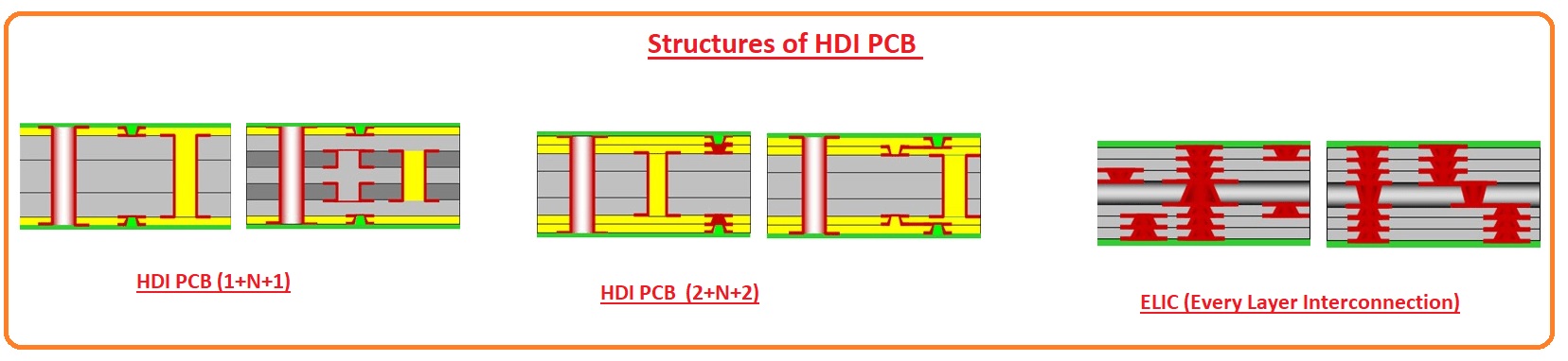
- Let us discuss them in detail.
HDI PCB (1+N+1)
- The type of the HDI printed circuit board comprises one build-up of larger density interlinking layers.
- It is the best option for BGA having fewer inputs and outputs.
- It comprises accurate lining micro via and registered techniques that have the capability of a 0.4-millimeter ball pitch.
- It provides high mounting stability.
HDI PCB (2+N+2)
- This category of HDI structure comprises of two or more two build-ups of larger-density interlinking layers.
- Micro vias at different layers can be staggered.
- This type of structure uses copper-filled stacked and is used in high-level applications.
- This structure is the finest for BGA having a small ball pitch and a larger no of inputs and outputs.
- It is used in such applications where routing density increment is required.
ELIC
- It stands for Every Layer Interconnection every layer of this PCB is largely density interlinking that permits conductive material at the layers of board to link to the copper-filled stacked micro via structure.
- It provides a highly reliable interlinking for complicated modules having larger numbers of pinouts like CPU, GPU, etc.
Benefits of HDI PCB
- The feature that make it useful are packaging density that is provided by the HDI technique.
- In this board room for the accurate trach, structures exist to different types of elements to connect.
- As this board provides net board size reduction so small size board will be constructed that is good for creating large projects.
- In general FPGA (field-programmable gate array) exists having one millimeter or less space.
Features Enhanced with HDI PCB:
- The common features important to the HDI is described here.
- It provides denser trace routing.
- The stability of power provided by this board is larger.
- It decreases the interference inductance and capacitance factors.
- In large-speed designing, it enhances signal integrity.
Accelerate Production with HDI PCB
- With this board, the linking of SMD devices is very easy than with other types of board.
- It provides high-speed routing.
- It also offers decrement in position replacement of components.
- There is a large space for more elements it has.
PCBWay HDI PCB manufacturing capabilities
- The features or capabilities provided by the PCBWAY in HDI PCB are discussed here.
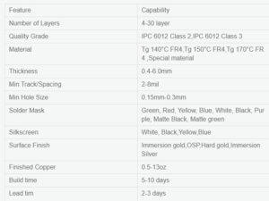
| Features | Capabilities |
| Number of Layers | Four to thirty layers exist in the HDI boards created by the PCBWAY. |
| Grade Quality | The grade quality provided by the PCBWAY is IPC 6012 Class Two and IPC 6012 Class Three. |
| Material | The common material used for HDI construction is Tg 140 centigrade FR4,Tg 150 centigrade FR4,Tg 170 centigrade FR4. |
| Board Thickness | The board is thickness has a value of 0.4 to 6 millimeters. |
| Minimum Track | The value of minimum spacing is 2-eight mil. |
| Minimum Hole Size | The dimension of the minimum hole is 0.15 milliliter from 0.3 millimeters. |
| Solder Mask | The Tsolder masks used in this technique are Green, Red, Yellow, Blue, White, Black, Purple, Matte Black, Matte green. |
| Silkscreen | The silkscreen is White, Black, Yellow, Blue |
| Surface Finishing | The surface finish used in PCBWAY are Immersion gold, OSP, Hard gold, Immersion Silver |
| Finished Copper | The finished copper is 0.5 to 13 ounces. |
| Creation time | It takes five to ten days. |
| Lead time | The lead time is two to three days. |
Credit to PCBWAY
What is the difference between HDI PCB and standard PCB?
- HDI boards are made with a larger number of micro-buried blind vias and normal PCBs are made with mechanical method drilling. HDI PCB drilled with laser. The number of layers and aspect ratio of the HDI board is increases.
What are the advantages of HDI PCB?
- The use of HDI PCB is important, and provides a more compact footprint and also has good electrical performance and high-speed transmission.
- It also supported more input and output of smaller geometries.
That is all about HDI PCB by PCBWAY Best PCB Supplier if you have any queries ask in the comments. Thanks for reading. Read our more Engineering Blogs