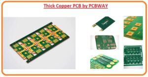
 Hi readers I hope you all are doing great. In this post, we will have a detailed look at Thick Copper PCB by PCBWAY. PCB full form is a printed circuit board and it most commonly used electronic circuit board over which circuits related to engineering and technical projects are assembled. At this board, different layers of coppers are designed over which different symbols of components are assembled to create different circuits.
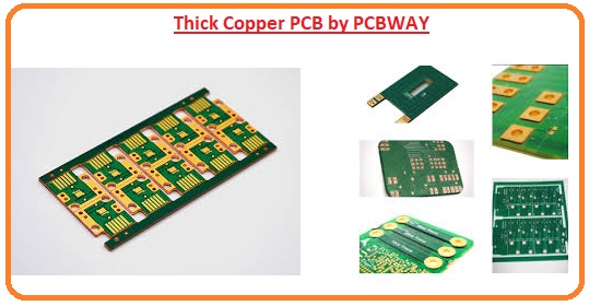
There are different categories of PCB such as single layer PCB, double layer PCB, multi-layer PCB, etc. PCB nowadays has become a very important part of our electronic engineering and project related to electronics. To make a good project by using PCB there is a need of high-quality PCB for this you must have to visit a PCB supplier that provides high-quality PCB at affordable prices. The supplier that I am suggesting to you is PCBWAY. It is the most famous PCB supplier that supplies its products all over the world. There are numerous services it provides related to PCB such as PCB prototyping, PCBA, etc. In this post, I am to going explain about their product which is thick copper which will help to you to avail of this product of this PCB supplier. So let’s get started with Thick Copper PCB by PCBWAY
What is Thick Copper PCB
- The thick copper PCB is also called heavy copper PCB or thick copper printed circuit board is a category of PCB that consists of a layer of copper having a thickness of three ounces per square foot at the inner and outer sides.
- Such PCB that has two ounces per square foot layer of copper is considered as the standard value of copper thickness and PCB having a layer of copper of four ounces per square foot thickness is called thick copper or heavy copper PCB board.
- During the construction of thick PCB, it is taken into consideration the weight and thickness of copper it define the current-carrying capability of PCB.
- This type of PCB has the ability to remove the wired bus arrangements. And it also permits the plating of a heavy copper at certain areas to work as a heat sink.
- This PCB board has the ability to show resistance against the large value of temperature.
Features of Thick Copper PCB
- The main features of thick copper PCB are described here with detail. Let’s discuss them one by one.
Large current Conduction
- This PCB board is used in such electrical industries where a large value current is used to operate different machines.
- To avoid the current cut pre-maturing this board is linked with other types of board..
- It provides high current carrying ability.
Good Thermal Distribution
- The copper-plated vias of this board provide high resistance related to thermal capability.
- Its continuous operation and ability to manage thermal variation make it useful for different products.
- Its temperature capability is such good that it can be used in such applications where the temperature is varying on a regular basis.
Implementation in Complicated Switching
- In this type of PCB board there is the absence of complicated wire connections and metallic bars. It creates a product that is less complicated and has less weight.
High Mechanical Strength
- This board has high mechanical strength that makes it robust and working for a long time.
Usage in Such applications Where high Power loss occurs
- The overheating process in the electrical system is very dangerous and can cause very serious problems.
- So the usage if this board makes it a reliable and easy process for you.
- With the use of this board, the temperature can be retained in the system according to the desired level.
- All this happening is due to the high heat dissipation capability of thick copper.
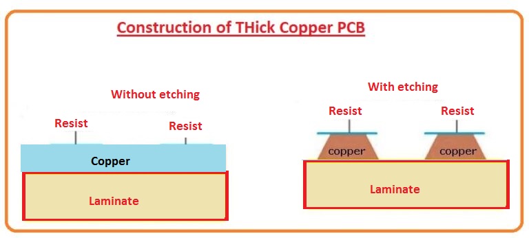
Construction of Thick Copper PCB
- There are most commonly used two techniques for the construction of Thick copper PCB first one is etching and the second one is plating.
- The main point taken into consideration during construction is to add the thickness of copper through plated holes and sidewalls.
- Point to remember is that the strength of the paired hole will be decreased when PCB follows numerous cycles during the fabrication process.
- After addition, the heavy copper strength of the holes increases.
- These features make it useful for such an application where a large value current is required.
- If you are constructing such a thick PCB that has a thickness of one hundred-five millimeters then you will have to face some problems. These issues are generally with a solder mask.
- At the substrate material due to restriction to the thickness of ink. The spraying process can not be used,.
- Nowadays two common methods are using in different industries. First is the usage of numerous solder mask prints.
- The second is to create a substrate first and then fill it with a solder mask,.
- after that use general PCB board solder resistance.
- With that printing, the screen causes some problems such as the breaking of soldering bridges, solder welding holes.
The below figure constriction process is discussed.
- The technique that uses thick mosaic etching uses a factor known as undercutting. Here the width of the circuitry path decreases.
- In these figures the are that is denoted with resists is the protecting layer that is photopolymer at single-layer board.
- It is mostly used at the end of the galvanic coating technique for double-layer or multilayer board.
Assembly Process of Thick Copper PCB
- The assembly processing of this board is described here.
- First of all, you would have a solid sheet of copper.
- After it must get laminated with the fiberglass sheet to make sure that it has a uniform thickness.
- Then do the drilling at the PCB board.
- Start plating of copper it done to do the plating of the inner side of drilled holes.
- It dependence is on the number of layers and sequence of laminated layers.
- If you do plating process before the etching than copper-plated will be connected again.
- The plating process is selective. It means it occurs at a certain place of the board.
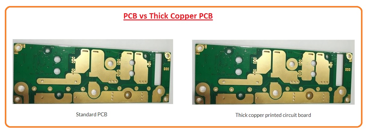
PCB vs Thick Copper PCB
- Now we do some comparison between standard PCB and thick copper PCB.
- Normal PCB either of which type it has can be created with the use of copper etching and plating process.
- Circuit layers are generally started with thing foil sheets of copper. To avoid undesired copper, these are etched.
- There plating is done to add copper thickness in the plans traces and pads.
- All circuitry layers have lamination to having net casing by using the epoxy-based substrate such as FR4.
- The construction process of heavy copper is the same as discussed above.
- But they are created with the use of etching and plating techniques. These techniques also comprise of high-speed plating.
- In previous years these features of copper were created with the use of an etching thick copper clade.
- In new techniques, thick copper is created with the use of a plating and etching combination.
- This causes the sidewalls and undercuts.
Applications of Thick Copper PCB
- The most common applications of thick copper PCB are described here.
- It used in military and defense systems for controlling weapons.
- It has the ability to the transformation of heat so it used in different electronic projects.
- It is used in the computer motherboard.
- It is used in automotive industries such as in rail track system and signal transmission system.
- It used in planer transformers.
- It used in pulse converter.
- It used in solar panels.
That all about Thick Copper PCB by PCBWAY I hope you must enjoy this post if you have any queries ask in the comments.


