This post will teach what QFN packages are—structure, types, processes, and functions. QFN packages are not important for electronics and semiconductors. QFN packages have made many changes to techniques used for the creation of ICs, like size, functions, and thermal features. In this post, we will discuss the details of QFn packages and find their types, structure, and functions. So let’s get started with What Are QFN Packages.
Introduction to QFN Packages
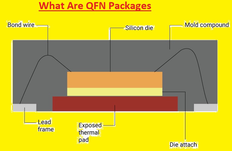
QFN is a leadless package that has a rectangular structure. Like the chip-level package, it is done with the use of a cutting machine.
A larger area exists for the exposed pad at the lower side for heat dissipation. It comes with a conductive pad for electrical connection on the surface with a larger pad.
QFN packages did not come with gull-wing leads such as SOIC and TSOP packages, so conductive paths between internal pins and pads are short and have low inductance with supplier resistance of wiring resistance in packages that offer good electrical features.
It also has good thermal operation through exposed lead frame pads with direct thermal paths for heat dissipation in the package. Normally thermal pads are connected on board, and thermal vias in the PCB help to spread extra power dissipation in the copper ground plan, which absorbs extra heat.
Due to its small size and weight having the best thermal features, this package is best for any application where size, weight, and operation are important.
Types of QFN Packages
Air-cavity QFN
- This package comes with a plastic or ceramic lid and copper lead frame and is open without a sealed plastic molded structure. Air cavity QFN packages are used in microwave systems with frequency values of 20 to 25 GHz.
Plastic molded QFN
- This type of QFN package is less costly than air cavity QFNs. It has a plastic compound and copper lead frame. These packages are used in 2 to 3 GHz frequency uses. There is no lid on plastic molded QFN packages.
Punch type QFN –
- It is molded in a single mold cavity format where different tools are used for operating the mold cavity.
Sawn type QFN –
- The molding process of this type of QFN, known as the mold array process, cut a larger number of boxes into small components.
QFN with wettable flanks
- It helps to visually check that the pad is configured on board through elevation given by wettable flanks.
Flip-chip QFN
- The cheap molded package is provided by flip-chip QFNs. This package employs flip-flop interconnection to make connections.
Wire bond QFN –
- This package has wire for the connection board to chip terminal.
Manufacturing QFN Packages
- First, there is a need to start assembly with solder paste printing. Then start spreading solder paste uniformly on the board before connecting the components.
- Now mounting QFN IC components on board according to board design. So it is important to use accurate tools for component placement since components come with high interconnection density.
- No pre-reflow inspection that makes sure that the board is fit to enter the reflow oven. When you start it, make sure that the board does not come with contaminants on the surface that can affect the soldering process.
- Now put the board in the reflow oven for soldering after confirmation that the board has a good structure.
- Now inspect the board after the reflow soldering process, which helps to find the soldering quality. It is important to note that there is a need for stencil design and a good PCB footprint for components connected.
Functions of QFN Packages
The main function of QFN packages is to connect the silicon die of integrated circuits with the PCB board.
QFN Packaging Process Flow
- Die Preparation
- Die Attach:
- Wire Bonding:
- Mold Encapsulation:
- Lead Frame Trimming:
- Marking and Inspection:
- Solder Plating:
- Testing:
- Tape and Reel Packaging:
Problems with QFN
Manufacturing Issues
The main concern with this package is manufacturability. It can be difficult to come up with a decreased defect rate in putting and reflowing QFN.
QFN comes with good features when used for low-mix, high-volume products. But it has some problems with high-mix, low-volume operations. This problem covers two points: board and stencil design.
So, for the stencil design process, there is a need to be accurate with the aperture design and stencil thickness. Such as if there is high voiding or passes exist, it will affect stencil design. The best technique is to follow manufacturing details. The solder thickness must be about two to 3 mils.
The aperture ratio of the pad must be 0.8:1 with many smaller apertures. For board design, the bond pad design must be about 0.2 to 0.3 mm away from the package footprint.
Soldering Problem
It is a chance of solder bridging due to the packages’ narrow pad-to-pad pitch. So the QFn does not come with a lead. So we have to face difficulty desoldering the package.
Advantages of QFN packages
- It is a less costly package.
- It does not have lead coplanarity problems.
- It provides good electrical performance.
- It comes with small-footprint mount instruments and flows for PCBA.
- It has a slight package lead inductance.
- It is a thin package and has less than one millimeter of package height.
- Due to the small size, board components can be close to QFN components due to the small size, location, and form factors of contact pads.
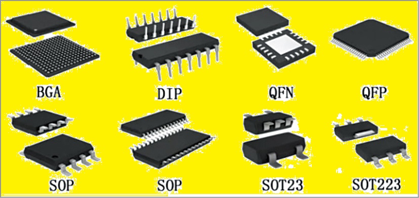
What is the difference between QFN and QFP?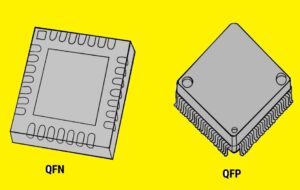
QFN
- It has leads extended on 4 sides of packages.
- It offers footing for packages during board assembly.
- It does not have variants.
- It has 8 pins and a thermal pad.
QFP
- In this package, pins are extended in an L or gull wing shape.
- It has a good base for the package during PCB assembly.
- Its main types are thin QFP (VQFP), low-profile QFP (LQFP), thin QFP (TQFP), etc.
- It has different pins, from 8 to 70 pins per side.
If you have limited space on the PCB board and a compact size is needed, QFN packages are best to use since they do not have leads and have smaller footprints.
If components need high pin numbers and larger lead spacing, QFP packages will be the best option.
QFN Packaging Process Types
ANVIL singulation:
- This package is defined based on stamping and cutting external lead wire with a die. Due to resin sealing of every cavity, the pins of packages are stamped with a die. As pressure is cut off, there is a short protruding xd pin on packages.
SAW singulation:
- This package comes with a rotary blade for cutting. As a package sealed in the same cavity is cut off through a rotary blade, the need face is like a pin end face side of this package.
Read also:
- Integrated Circuits (ICs) definition, Working, Types & Applications
- Matte vs Glossy in PCBs
- Lead vs. Lead-Free Solder in PCB Manufacturing – 2023 Ultimate Guide
- PCB Heat Dissipation Techniques
- The Importance of Copper Pour in Empty Areas on PCBs
- What is PLCC Packages | SMD Plastic Leaded Chip Carrier – How Do We Use Them?
Faqs
Why is the QFN package used?
- It is an IC component used for microcomputers and programmable modules. It is suggested to use for PCBs designed with size, thickness, and weight-related parameters.
Lead vs. Lead-Free Solder in PCB Manufacturing – 2023 Ultimate Guide
What does the QFN package stand for?
- The QFN package is used due to its compact size, good electrical and thermal features, and lower cost. Its small footprint and thin profile make it best for compact devices where space is important.
What is the difference between QFP and QFN packages?
| Feature | QFP | QFN |
| Pins | 32 to more than 100 | Less than 32 |
| Lead pitch | Small | Large |
| Leads | used to connect the package to the board | No leads connected to PCB with SMT |
| Size | larger than QFN packages | smaller than QFP packages |
- What is the name of the QFN package?
- QFN’s full form is quad flat no-lead package. The main parts of QFN packages are the lead frame, single or many dies, wire bonds, and molding compounds.
What are BGA and QFN?
- BGA has a larger pitch than QFP; BGA components are easily connected, so relatively high efficiency is provided. For defects concerning packages tested before assembly, the assembly failure rate can be lower than 1 ppm.
What is the price of QFN IC?
- The cost of QFN ICs depends on size, complexity, and manufacturer. However, QFN ICs are more costly than other types of IC packages, like SOIC and DIP.
What are the disadvantages of the QFN package?
- limited heat dissipation:
- Complex Assembly Process
- Limited Accessibility for Testing and Debugging
- Sensitivity to Mechanical Stress:
- Difficult PCB Rework:
What is a son package?
- SON stands for small outline no-lead.Small Outline No Lead offers a small form factor at 0.4 and 0.5 mm pitch. There are fewerr pin-count devices in plastic packages supported with equipment, including automotive
What is the most popular IC package?
- Dual-in-line Package (DIP) is commonly used through-hole IC packages in circuits, especially used for hobby projects. It comes with 2 parallel rows of pins at 90 degrees out of the plastic casing. Its dimensions are based on pin count.
Which IC is best for the inverter?
- In an inverter, 220 volts can be obtained with the use of IC 4047 and 4011.
What are the 2 basic types of IC?
- Digital Integrated Circuit.
- Analog Integrated Circuit.
- Mixed Integrated Circuit.
What is a QFP IC package?
- The quad flat package is a surface-mounted integrated circuit package with gullwing leads that exist on 4 sides. Socketing these packages is rare, and through-hole mounting is not possible. Normally, connectors with 32 to 304 pins and a pitch ranging from 0.4 to 1.0 mm are common.