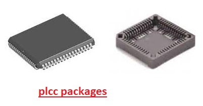
PLCC packages are integrated circuit packaging that protects sensitive components in a protective casing. These packaging are created to protect integrated circuits by providing easy installation on the PCB board. The PLCC full form is a Plastic Leaded Chip Carrier. This packaging comes in a rectangle or square structure, and pins are extended out from their sides. This packaging comes with normally twenty to eighty-four pins or more according to applications.
Types of PLCC Packages
Standard PLCC
The Standard PLCC is the quintessential part of the PLCC group. it comes with a square structure and a larger number of pins and is part of electronic projects. its square layout offers a balance between space used and easy handling during installation. These PLCC packaging are mostly used in devices where size restrictions are not important to help to make complicated circuits with the use of a larger number of pins
Applications: This packaging is mostly used in memory modules, microcontrollers, and different consumer electronics. Their versatile structure and larger pins make them best to be used in different projects
Miniature PLCC
Miniature PLCC is a compact type of PLCC package. This small-size packaging is made for applications where space is important without compromising circuit function. In spite of their small size, these PLCCs provide good electrical and thermal performance, making them best for devices that have limited space.
Applications: These packages are used in space-constrained applications such as wearable devices, portable electronics, and medical instruments. Their main feature to pack substantial functionality in a small form factor makes them preferable for these devices
Thin Quad Flat Package (TQFP)
The Thin Quad Flat Package type provides a different design perspective to the PLCC packaging. By providing the protection dn benefits of the PLCC series this packaging offers a flatter profile, while minimizing the overall weight. This design layout increases its feature to dissipate heat effectively which is an important parameter for devices that involve high power
Applications: TQFP packages are employed in digital signal processors, microprocessors, and graphics cards. The enhanced heat dissipation makes them preferable packaging for devices that need significant computational power.
Enhanced PLCC
For projects that need an extra layer of performance, the Enhanced PLCC can be used. These packages have some extra features, like additional heat sinks, or optimized thermal paths. By handling the thermal issues and improving overall performance, enhanced PLCC packages handle high-performance conditions.
Applications: These PLCC packages are used in graphics-intensive tasks, high-speed data processing, and applications that need a consistent and reliable operation for longer duration
Ceramic PLCC
With the use of ceramic material, the Ceramic PLCC offers changes from the conventional plastic body. Ceramics provides good thermal conductivity and durability and makes this packaging best for projects that need good heat dissipation and mechanical strength. This type of PLCC is used in industrial devices and high-power electronics
PLCC vs. DIP
Aspect | PLCC | DIP |
---|---|---|
Physical Design | It has a Square or rectangular shape with leads about the perimeter. | it has a rectangular shape with 2 parallel rows of pins extending from opposite sides. |
Pin Count | it has larger pinouts than DIP packaging and is employed in complicated circuits | it has less pinout and is mostly used in simple projects |
Space Efficiency | Compact design, good for space-constrained devices | it is heavyweight due to wider pins spacing, potentially taking up larger board space. |
Heat Dissipation | it provides enough heat dissipation, especially for enhanced PLCC packages. | it provides limited heat dissipation since it needs additional heat sinks |
Ease of Handling | its pins are sensitive due to its small size and closer spacing | it has strong leads that make handling easy during installation and testing. |
Applications | it is mostly used in the automobile industry, consumer electronic devices | it is a conventional option for prototyping and simple circuits. |
Prototyping | Due to the closer lead spacing, soldering PLCC packages can be challenging. | DIP packages can be easily prototyped and tested which makes them good for development. |
Cost-Effectiveness | it is less costly due to its versatile nature and compact design | Economical is good for simple designs and larger pinout pitches. |
Retrofitting | Replacement or upgrading PLCC packages can need more work due to the compact size | Replacement is relatively easier due to the large size and lead spacing |
PLCC vs. BGA
Aspect | PLCC | BGA |
---|---|---|
Package Design | Square or rectangular shape | a collection of solder balls on the underside frequently exists under the container. |
Pin Count | it has a Moderate to larger number of pins | it pins count changes from moderate to very high, making them best for complex and high-performance designs. |
Space Efficiency | it has a compact layout and there is effective use of space in that design | There is effective space due to solder ball configuration and it provides smaller package sizes. |
Heat Dissipation | It has enough heat dissipation and can need extra heat sinks for high power. | it has Efficient heat dissipation due to the larger surface area of solder balls. |
Manufacturing | Its manufacturing process is simple and best for automated assembly | The complicated manufacturing process comes with precise ball configuration and soldering techniques. |
Durability | it is sensitive to mechanical stress and can need more precision during handling | Resilient against mechanical stress since it did not have leads and uses of solder balls |
Applications | Industries and consumer electronics | it is commonly used in high-performance applications like GPUs, CPUs, and networking devices |
PLCC Package features
- Compact Design: PLCC packages are made to increase space efficiency. They come with a compact outline that is used for high-density packaging of ICs on printed circuit boards, making them a good option for devices that have limited space.
- Leaded Configuration: These packages come with pins that are extended out from their sides. This structure makes simple PCB design and offers different points for connection and increases signal quality and makes the soldering process easy
- Easy Handling: Their pins or leads helps this packing to handle easily during manual assembly and automated pick and place process. Leads help to easily configure and connect packaging on the board.
- Versatility: There are can the larger number of ICs can be configured on this package like analog and digital circuits, controller memory chips, and other components. This feature makes them best for applications from small electronic devices to industrial uses
- Thermal Performance: During the creation of this packaging there is thermal parameters are considered. Different PLCC packaging comes with thermal pads or exposed metal surfaces on the inner side that easily dissipate heat produced by an enclosed integrated circuit. Enhanced PLCC packaging offers good thermal operation for power-intensive projects
- Reliable Electrical Connections: The leaded structure of PLCC packaging provides reliable electrical connections between the Integrated circuits and the external circuits. The leads are properly spaced and configured, reducing the chance of electrical short circuits or improper connections.
- Environmental Protection: PLCC packages provide a protective layout for the enclosed circuits, protecting them from different parameters like dust, moisture, and contaminants. The plastic mold compound offers a barrier that decreases the operating life of the integrated circuits
- Compatibility with PCB Manufacturing: These packages are made to be supported standard PCB manufacturing processes, like through-hole technology. and surface mount technology. This compatibility makes the assembly process easy and minimizes manufacturing complications
- Upgradability: PLCC packages are used for easy elimination and change of the ICs, making them good for applications where maintenance is needed. This feature is good and preferred in industries where changes in technology are needed
- Cost-Effectiveness: Due to their effective design and manufacturing methods, PLCC packages provide cost-effective solutions for configuring ICs, making them good options for both electronics and industrial projects.
- Ergonomic Handling: Some PLCC packages come with chamfered or rounded corners, which not just increases the appearance but also makes them ergonomic to handle during assembly and connection
Construction of PLCC Package
- Lead Frame Fabrication: The PLCC manufacturing process started with the creation of a lead frame that works as the base of the packaging. The lead frame is normally created with metallic alloys like copper or alloy. The lead frame comes with a central die page where the IC chip is mounted and the leads are extended in an outward direction. After that, these leads will be configured with outer circuits
- Die Attach: In this step there is the connection of IC chips is made with the die pad of the lead frame. It is mostly done with the use of die-attached adhesive, that is special epoxy resin that strongly holds the chip in position with providing the thermal conductivity for heat dissipation. The IC chip is properly aligned and the positioned on die pad with the use of accurate machines
- Wire Bonding: When IC chips are connected wire bonding is done to make an electrical connection between the the pads of chips bond and the pins of the lead frame. A thin wire is created with materials of aluminum or gold used for wire bonding. The wire bonding machines use ultrasonic energy to connect wires to make sure reliable electrical connections.
- Mold Encapsulation: After completion of wire bonding assembly is enclosed in a plastic mold compound. This compound is a thermosetting resin that offers mechanical protection, environmental conditions, and electrical insulation for sensitive IC chips and wire bonds. The mold compound is normally applied around the lead frame and the IC chip cover wire bonds and most parts of the lead frame.
- Curing and Trimming: The encapsulated assembly goes to the curing process where the mold compound becomes solid and makes a protective shell around the IC. Extra mold compound is removed through trimming to show pins and make sure they are ready for the soldering process during board assembly
- Lead Forming: After cutting, the leads extend from the PLCC package and become straight. It can be done with the use of automated lead creation instruments to ensure consistent lead structure for accurate soldering on board
- Testing and Inspection: Quality control is important for PLCC package manufacturing. Comprehensive testing and inspection processes are done to check the quality of electrical connections, wire bonds, and package dimensions. Automated instruments check for insulation resistance electrical continuity, and other main parameters.
- Marking and Labeling: PLCC packages have markings or labels to show important information like manufacturer logos, part numbers, and orientation indicators. These markings are normally laser-etched or ink-printed onto the packaging surface.
- Tape and Reel Packaging: When the PLCC packages complete quality assurance, they are normally packaged in tape and reel format for easy handling during board assembly. The packages are configured pockets on a continuous tape, which is wound onto a reel. This packaging layout helps the effective automated pick-and-place assembly on the board.
- Final Inspection and Packaging: Before distribution, a final inspection makes sure that the packages are according to needed standards and specifications.
PLCC Packages and Troubleshooting and Repair
- Inspect the Package: First of all PLCC packaging is thoroughly inspected visually. Check the packaging to find any damage like chips, cracks, or bend leads. Make sure the packaging is accurately seated on board and the leads are aligned properly.
- Test the Integrated Circuit: If it checks that PLCC packaging is faulty, then it is tested the integrated circuits. There can be accurate testing instruments such as logic analyzers or IC tests that can be used to assess the function of ICs. Confirm that IC is working as required and generating accurate output signals
- Check the Connections: There can be a malfunction of PLCC packages due to improper connections. Check the solder joints between PLCC leads and board pads. To check that there are no solder bridges, cold joints or other soldering faults magnifying glass or microscope can be used. Reflow soldering can be used to make proper connections.
- Replace the Package: If the packaging itself is found to be faulty, it can be replaced. Properly desolder the faulty packaging from the board with the use of a soldering iron or hot air rework station. After removing clean pads to be ready for installation of new packaging.
- Consider Professional Repair: Repairing packages can be a complicated process and can need certain instruments and experience. In some conditions, it is suggested that get the services of professionals to repair, especially for complicated ICs.