 Hello friends, I hope you all are doing great. In today’s tutorial, we will have a look at Common-Source FET Amplifiers Operation. There are three main types of configurations of FET like the BJT which are common emitter, common base, and common collector. The common source amplifier is the basic field-effect transistor technique that normally works as a voltage amplifier. The simple method to know configuration is either a common drain, gate, or source to find the direction of signal from it entering and leaving. The other terminal remains common.
For common source configuration signal enter in the gate and leave from the drain. While source is common between these two terminals this configuration is known as common source configuration. In today’s post we will have a detailed look at its circuit, working, and related parameters. So let’s get started with Common-Source FET Amplifiers Operation.
Common-Source FET Amplifiers Operation
AC Model of FET
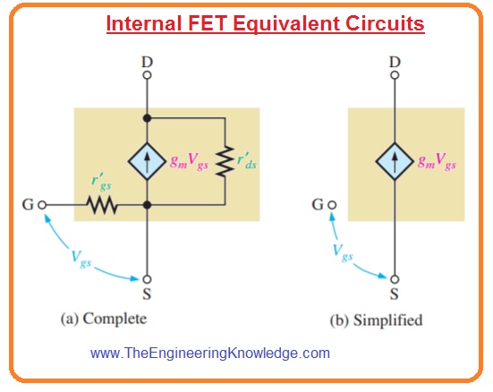
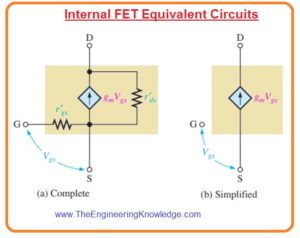
- In the below figure the resultant field-effect transistor model is shown.
- In figure denoted as ‘a’ the interior resistance exits among the gate and source and the current source is equal to the gmVgs that is existing among the drain and source.
- There is an internal drain to source resistance is exits.
- In figure denoted as ‘b’ simple model of FET is displayed.
- The resistance has large value due to there is open circuitry between the gate and the source.
- It is such a large value that can be ignored.
- In below figure the ideal field effect transistor circuitry model having exterior ac drain resistance is shown.
- The value of ac voltage gain of this circuitry is Vout/Vin, here Vin=Vgs and Vout=Vds.
- The equation of voltage gain can be defined as.
Av= Vds/ Vgs
- From the resultant circuitry we have.
Vds = IdRd
- According to the definition of transconductance we have.
gm =Id/Vgs
Vgs=Id/gm
- Putting value of Vgs and Vds in the voltage gain equation we have.
Av=IdRd/(Id/gm)
gmIdRd/Id
Av= gmRd—-(A)
JFET Amplifier Working
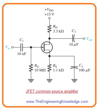
- The common source JFET amplifier configuration is shown in below figure in which ac voltage as input is provided at the gate terminal and ac output is taken from the drain terminal.
- In this configuration, the source is common among the input and output voltage signal.
- The common source amplifier configuration sometimes has no source resistance or has bypassed source resistance therefore source is attached with the ac ground.
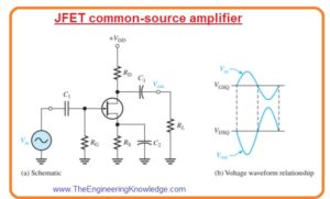
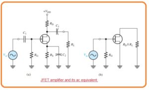
- The self-biased common source N channel junction field effect transistor amplifier configuration with the ac source capacitively coupled with the gate is shown in the below figure denoted as ‘a’.
- There are 2 main functions of resistance RG first is it keeps the gate at 0 volts dc since IGss is very less and it high value normally in megaohms stops the loading of ac signal source.
- The bias voltage is generated due to voltage loss about resistance RS.
- Due to the bypass capacitor, C2 source of JFET is at ac ground.
- Due to the input signal gate to source voltage move over its Q-point value (VGSQ), that causes the resultant swing in the drain current.
- With the increment in drain current the voltage loss about resistance RD also increases which causes the drain voltage to decrease.
- The drain current moves across its Q-point value in phase with the gate to source.
Graphical Representation
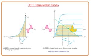
- The function above explained for n channel junction field effect transistor is graphically shown on both transfer characteristic curve and drain characteristics curve in below figure.
- The figure denoted as ‘a’ shows a sine waveform-like changing, Vgs generates a resultant ac signal changing in the current Id.
- With the movement of Vgs above its Q-point value to negative value current Id reduces from its Q-point value.
- When Vgs moves to less negative value current Id increases.
- The figure denoted as ‘b’ shows the similar function with the drain curves.
- The voltage signal at the gate runs the drain current over the Q-point on load line as denoted with the arrows.
- Lines drawn from the peak of gate voltage to the ID axis and to the VDS axis denoted the peak to peak changing of drain current and drain to source voltage as display in figure.
- As the transfer characteristic curve is nonlinear there will be some distortion in the output.
- It can be reduced if the signal moves over the restricted part of load line.
JFET Amplifier DC Analysis
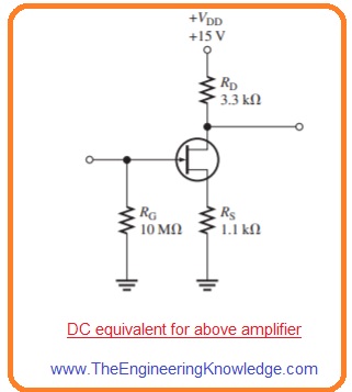
- To analyze JFET amplifier first step is to find the dc parameter consisting of drain current ID and VS.
- Current ID find the Q-point of amplifier and help to find the value of VD therefore it is beneficial to find its value.
- It can also calculate through graphical representation or mathematically.
- For simplification of dc analysis the resultant circuitry is shown below where capacitor are appearing open to dc therefor are eliminated.
AC Equivalent Circuit of Amplifier
- For analysis of signal operation of above-given amplifier we make an ac resultant circuitry.
- For this substitute capacitor with the short circuits, according to the simplification based on the signal frequency.
- Substitute the dc source with the ground by considering that voltage source has 0 value of internal resistance.
- The VDD terminal is at 0 volt ac level and so behaves like an ac ground.
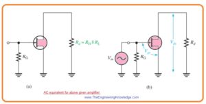
- the ac resultant corresponding circuit is shown in below figure denoted as ‘a’.
- Not that +VDD end of RD and source terminal are at ac ground.
- According to ac analysis the ac ground and actual circuitry ground are working as a similar point.
Signal Voltage at Gate
- In figure denoted as b ac voltage source is shown attached with the input.
- As input resistance of JFET has large value, in practice all input voltage from the signal source exits at gate terminal with less voltage loss at internal source resistance.
Vgs = Vin
Voltage Gain
- The equation of voltage of JFET which is given in equation A is applied to common source amplifier.
Av =gmRd
- The output signal voltage VDs at drain will be.
Vout = Vds = AvVgs
or
Vout = gmRdVin
- In this equation
Rd = RDΙΙRL and Vin = Vgs.
Effect of AC Load on Voltage Gain
- When load is attached with the output of the amplifier through the coupling capacitor as shown in figure denoted as ‘a’.
- The ac drain resistance RD is in parallel with load resistance RL since the upper part of RD is at ac ground.
- The resultant circuitry is shown in the figure denoted as ‘b’.
- The total ac drain resistance will be.
Rd=RDRL/(RD + RL)
- The effect of load resistance is to decrease the unloaded voltage gain.
Phase Inversion
- The output voltage taken at the drain is out of phase or 180 degrees with the input voltage at the gate terminal.
- The phase inversion can be denoted through the negative voltage gain.
Input Resistance
- Since the input to common source amplifier is at the gate the input resistance value is very large.
- In ideal it equal to infinity and can be ignored.
- As we know that the large input resistance is generated by the reversing biasing pn junction in the junction field effect transistor and through the insulated gate structure in MOSFET.
- The real resistance observed by the signal source is the gate-to-ground resistance RG in parallel combination with the input resistance of FET VGS/IGSS.
- The reverse leakage current IGSS is normally mentioned on the datasheet for a certain value of VGS so that the input resistance of module can be found.
Rin=RGΙΙ(VGS/IGSS)
- As the term (VGS/IGSS) larger than the RG the input resistance is almost close to the value of resistance RG.
D-MOSFET Amplifier Working
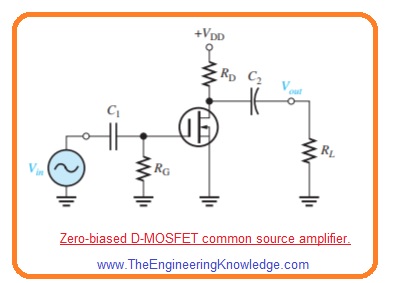
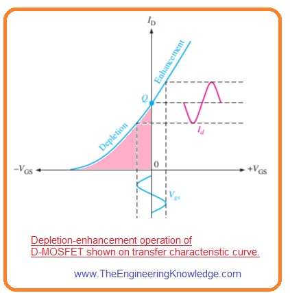
- In below figure the zero biased common source n channel D MOSFET with coupled with ac source through capacitor to the gate is shown.
- The gate is almost zero volts dc and source is at ground which make VGS=zero volts.
- Due to signal voltage source Vgs move over its 0 value causes swing in current Id as shown in figure.
- The negative swing im value of VGs generates the depletion mode and current Id reduces.
- The positive swing in VGs generates the enhancement mode and current Id enhances.
- You can see that enhancement mode is at right side of vertical axis or VGS=0 and depletion mode is on the left side.
- The dc analysis of the amplifier configuration is easy then the junction field effect transistor since ID=IDSS at VGS=0.
- When current ID is known the analysis gives only value of VD.
VD = VDD – IDRD
E-MOSFET Amplifier Working
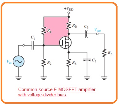
- In the below figure common source n channel E MOSFET with voltage divider bias configuration with ac source capacitively coupled to the gate is shown below.
- The gate is biased with a positive voltage such that VGS>VGS(th).
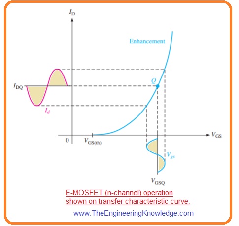
- With the JFET and D MOSFET the signal voltage generates a swing in VGs over its Q-point value VGSQ.
- It generates a swing in value of the current Id over its Q-point value IDQ as shown in below figure.
Read also
- Introduction to JFET (Junction Field Effect Transistor)
- Transistor Symbols | Definition, Terminals & Operating Condition
- Difference between Vacuum Tube and Transistor
- Introduction to BC108 NPN Transistor
- What is Optocoupler,Working, Types & Applications
- Audio Amplifier Circuit
- Introduction to MPSA06 NPN Amplifier Transistor
So friends that is a detailed post about Common-Source FET Amplifiers if you have any questions ask in the comments. Thanks for reading. Have a good day.
