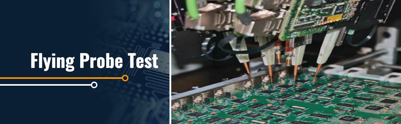
Hi guys welcome to the new post. In this post, we will learn What is a PCB Flying Probe Test. The durability and quality of PCB boards are crucial in the quick-paced world of electronics manufacturing. As PCBs become increasingly complicated and densely packed with components, traditional testing techniques like manual testing and bed-of-nails testing have some limitations in terms of time, cost, and test coverage. This is where the PCB flying probe test comes to use, offering a flexible and effective solution for testing PCBs in 2023. So let’s get started Introduction to flying probe testing
Understanding PCB Testing
Before discussing the details of the PCB flying probe test, it is necessary to understand the shortcomings of traditional testing techniques. Manual testing, which entails checking the board visually for flaws, takes time and is prone to human mistakes. Bed-of-nails testing, while, need the fabrication of a custom fixture, making it costly and unsuitable for complicated PCB designs.
Introduction to PCB Flying Probe Testing
A flying probe tester is automated PCB testing that reduces the limitations of traditional processes. It uses specialized equipment, like pair of robotic probes, to access the electrical nodes of a board and perform many tests. The probes move swiftly about the board, making contact with certain test points to find electrical features and detect any potential faults
Advantages of PCB Flying Probe Test
The main advantage of the PCB flying probe testing technique is its flexibility and adaptability. Unlike bed-of-nails testing, which needs the fabrication of a custom fixture for every PCB design, flying probe PCB testing does not base on a fixed fixture. This makes it suitable for prototyping and low-volume production where time and cost are critical factors.
Furthermore, the PCB flying probe test offers cost-effectiveness. The absence of a custom fixture reduces setup costs, making it a viable option for small-scale manufacturing. With that, the ability to test many PCB designs without varying the setup saves both time and money.
Time efficiency is also the notable advantage of the flying probe circuit board testers, With no use of fixture fabrication, the setup time is significantly decreased. The automated nature of the test further speeds up the process, making it good for time-sensitive projects.
Moreover, the flying probe pcb test is capable of testing complicated board designs with fine-pitch components and high-density interconnect boards. The flying probes can access tight spaces and small testing points, ensuring good test coverage.
Applications of PCB Flying Probe Test
This test is suitable for a variety of applications because of its adaptability. It is helpful in low-volume manufacturing and prototyping, when the capacity to swiftly set up and test several designs is required.
HDI PCBs, which are characterized by high component density and many layers, can also benefit from flying probe tests. The probes can accurately access fine-pitch components and test the intricate PCB structure’s connectivity.
Furthermore, this test is advantageous for multi-layer boards where access to inner layers is limited. The probes can navigate through the board, making sure that all layers are thoroughly tested.
Boards with fine-pitch components, like those found in consumer electronics and communication devices, can also be effectively tested using the flying probe method. The probes make accurate contact with these small test points, offering reliable test outcomes
Challenges and Limitations of PCB Flying Probe Test
As this test offers many benefits, it also has its limitations. It can not detect different types of defects, like intermittent faults that exist under certain conditions. With that, false negatives can occur if the test setup is not correctly optimized or if the probes do not make sufficient connections with the test points.
Another limitation is the test coverage. As the probes move sequentially and make connection with each test point individually, the net test time can be larger compared to other techniques like in-circuit testing (ICT) or automated optical inspection. So, it is significant to carefully consider the test plan and optimize the testing point selection to make sure maximum coverage.
Best Practices for PCB Flying Probe Test
To get optimal results with PCB flying probe tester, differnt best practices must be followed. Firstly, design considerations are important. By designing a board with accurate testability in mind, like test points, and avoiding excessive vias, the flying probe testing becomes efficient and accurate.
Optimizing the testing points is also necessary. By strategically choosing the test points and considering factors like component accessibility and test coverage, the test time can be reduced while maintaining thorough testing.
That, developing a comprehensive testing plan is important for successfully flying probe PCB test. This involves defining certain tests to be performed, finding the order of test points, and setting up the pass/fail criteria. A well-defined test plan makes sure that all necessary tests are applied, decreasing the chances of overlooking potential defects.
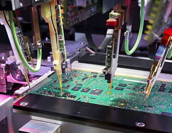
How Does Flying Probe Testing Work?
. Preparation
The first step in this testing is to prepare the PCB board. That is cleaning the PCB board, applying a solder mask, and adding test points. Test points are small pads on the board that the flying probe tester can use to make contact with the PCB
2. Programming
The 2nd step is to program the flying probe tester. This involves making a test program that tells the tester which test points to contact and what tests have to do. The test program is made using a software program that is offer by the flying probe tester manufacturer.
3. Testing
Once the PCB board is prepared and the test program is configured, the PCB board can be tested. The board is placed on a conveyor belt and the flying probe tester moves the probes over the board. The probes contact the test points and the tester does the tests that are specified in the testing program.
4. Results
The outcomes of the tests are shown on the flying probe tester’s computer screen. The results can be used to find any defects in the board
Flying Probe Testing vs. ICT Testing
Flying Probe Testing | ICT Testing (In-Circuit Testing) |
---|---|
Automated testing method | Automated testing method |
Utilizes robotic probes | It uses test fixtures and probes |
Does not need custom fixtures | It needs custom fixtures for each PCB board design |
Flexible and adaptable | Limited flexibility, needs dedicated fixtures |
Best for low-volume production and prototyping | Good for high-volume production |
Can test complicated board designs with fine-pitch components and HDI boards | Limited ability to test complicated designs |
Tests individual test points sequentially | Simultaneously tests multiple test points |
Longer test time due to sequential testing | Less test time due to simultaneous testing |
Cost-effective for small-scale manufacturing | Higher setup cost for fixture fabrication |
Can access tight spaces and small test points | Limited accessibility for certain components |
Comprehensive test coverage | Limited test coverage for some defects |
Detects defects like shorts opens, and component value variations | Detects defects like shorts opens, and component value variations |
No physical connection with PCB components | Physical contact with PCB board components |
Non-destructive testing method | Non-destructive testing method |
Does not need electrical power to the PCB board during testing | Requires electrical power to the board during testing |
Can be employed for functional testing in addition to electrical testing | Primarily focused on electrical testing |
WHAT KINDS OF PROJECTS WORK BEST WITH A FLYING PROBER?
Flying probe testers are a versatile testing technique that can be used to test differnt types of PCBs. They are frequently used for prototyping and low to mid-volume manufacturing, but under certain circumstances, they may also be utilized for high-volume production.
Here are some of the types of projects that work well with a flying prober:
- Prototypes: Flying probe testers are a good way to test prototypes fastly and accurately.As they do not need custom fixtures, which can be time-consuming and costly to make.
- Low-volume production: These tests are also a good option for low-volume production. This is due to that they are more cost-effective than other testing methods, like in-circuit testing (ICT).
- High-density boards: High-density boards: while they can be used to evaluate high-density boards, they may not always be the best choice.. This is due to that flying probe testers can be slower than other testing techniques like ICT.
Circuit Board Testers
Here commonly used circuit board testers, are listed
- In-Circuit Testers (ICT):
- Flying Probe Testers
- Automated Optical Inspection (AOI) System
- X-ray Inspection Systems
- Functional Testers
Conclusion
The PCB flying probe test has become a flexible and effective method for evaluating PCBs in the constantly changing field of electronics production in 2023. It is a vital instrument for guaranteeing the quality and dependability of PCBs due to its versatility, affordability, and capacity to test complicated designs. Manufacturers may take use of the benefits of the flying probe test to simplify their production processes by using best practises and improving the test procedure.
FAQS
What is the difference between flying probes and ICT testing?
The basic difference between flying probe testing and in-circuit testing (ICT) lies in the testing approach and equipment used. Flying probe testing uses robotic probes that move across the board to make connections with certain test points, while ICT needs custom test fixtures and probes to make electrical connections. Flying probe testing provides adaptability, flexibility, and the ability to test complicated designs without custom fixtures, making it good for low-volume production and prototyping. While, ICT is best for high-volume production and can simultaneously test many test points, resulting in shorter test times.
What is the FPT test in PCB?
FPT stands for Flying Probe Test, which is a type of testing technique used to examine boards (PCBs). In FPT, robotic probes are employed to make contact with the testing points on the board to find electrical features and detect any potential problems. FPT is also used for its flexibility, cost-effectiveness, and good for testing complicated PCB board designs
What is GPT vs FPT?
GPT or (Giant Perpendicularity Test) and FPT (Flying Probe Test) are 2 completely different concepts. GPT is defined as a testing method employed to determine the perpendicularity or alignment of properties or structures, generally in mechanical or engineering contexts. While, FPT is a testing process specifically used for board, where robotic probes are employed to make electrical connections with test points on the board
What is MPT vs FPT?
MPT (Manual Penetration Test) and FPT (Flying Probe Test) are diferent testing methods with different applications. MPT follows manually testing the hardness or resistance of a material’s surface by penetrating it with a specialized tool. FPT, while is an automated testing technique used for board, where robotic probes make contact with test points to find electrical parameters
Why is GPT used?
GPT, or Giant Perpendicularity Test, is employed to evaluate the perpendicularity or alignment of a feature or structure. It helps to make ensure that components or structures are accurately aligned according to certain tolerances. GPT is used in mechanical and engineering industries to check the accuracy and quality of parts, assemblies, or structures.
What is FPT technology?
FPT, , is a technology used for testing printed circuit boards. It involves the use of robotic probes that move across the board and makes contact with certain testing points to find electrical characteristics and detect potential defects. FPT technology provides adaptability, flexibility, and cost-effectiveness in testing different types of board
What does FPT mean in mechanical?
In a mechanical context, FPT’s full form is Fasteners Per Team. This refers to the number of fasteners (like screws, bolts, or nuts) needed for assembly or construction per team or group of workers.
What is FTP short for?
FTP full form is File Transfer Protocol. It is a common network protocol used for file transfers between clients and servers over a network of computers.. FTP enables the exchange of files in a reliable and effective way, moslty used for website maintenance, software distribution, and data transfers.