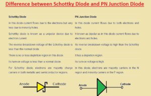
 Hello, readers welcome to the new post. Today we will discuss Difference between PN junction Diode and the Schottky diode. A diode is an electronic component that comes with two pinout anode and a cathode. Positive is called the anode and negative is called the cathode. The function of the diode is rectification where ac is converted into dc current.
The circuit where the diode performs the rectification is called a rectifier. In electronic various types of diodes used in this post, we will cover the differences between the PN junction Diode and the Schottky diode. So let’s get started Difference between PN Junction Diode and Schottky diode
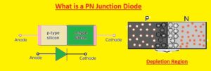
What is a PN Junction Diode?
- The PN junction diode is a two-terminal electronic component called a semiconductor component. Through this diode current passes in one direction is the forward direction and opposes in the reverse direction.
- If the diode is in forward biased state current passes through it and not current flows in a reverse-biased state.
- PN junction diode is also known as pn junction semiconductor component.
- The pn junction diode has P and N region n region has free electrons as majority carriers and P has holes as majority charge carriers.
- Through a combination of p and n region pn junction is created. The diode that hs PN junction is called the pn junction diode
- The PN junction diode is created through the use of semiconductor materials like silicon, germanium, and gallium arsenide.
- Mostly silicon material is used for the creation of diodes since silicon can bear high temperatures and operate well in these conditions
- When dc voltage is given to the diode in such configuration the positive terminal of the battery is connected to the anode and the negative to the cathode forward biased state of the diode is created and in opposite polarity reversed biased state created
- PN junction diode is used in switching and rectifier circuits
What is Schottky Diode
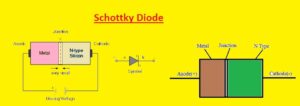
- In the PN junction diode, P and N materials are used to create a PN junction. The use of P and N materials created the PN junction
- While in the case of the Schottky diode metallic material such as aluminum or platinum is used in place of P material. The Schottky diode name was given due to German physicist Walter H Schottky
- This diode is also called the Schottky diode ,surface barrier diode or hot electron diode. it commonly used for RF circuits
- Schottky diode is a power diode that has higher voltage and current ratings than a normal PN junction diode
- In the case of forward biased condition, free electrons pass through a metal-semiconductor junction. As there is no hole exists in metals so for a forward biased stat, thee current is due to free electrons
Schottky Diode Working
- The working operation of this diode is based on the electrons existing in different materials with different potential energy
- The potential energy for the N region is higher than the metallic part
- When these two parts come closer to each other there is the movement of electrons in two directions about the metal and semiconductor region
- The voltage is provided in such a configuration that the metallic part is positive for the semiconductor part.
- The creation of potential is restricted by the voltage and current flows
V-I Characteristics of Schottky Diode
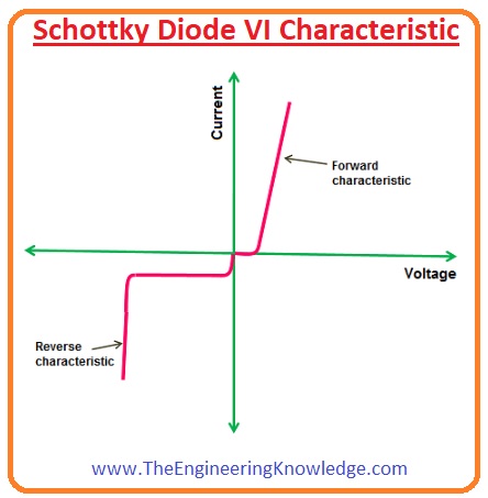
- The VI characteristics of the Schottky diode are like the PN junction diode. Current is a dependent variable and voltage is an independent variable for VI graphs. The value of the Schottky diode is about 0.2 to 0.3 volts
Difference between Schottky Diode and PN Junction Diode
| PN Junction Diode | Schottky Diode |
|---|---|
| Formed by joining a P-type and an N-type semiconductor | Formed by joining a metal and an N-type semiconductor |
| The junction between P and N-type semiconductors acts as a barrier to current flow | Schottky barrier between metal and semiconductor acts as a barrier to current flow |
| Larger depletion region, higher reverse leakage current | Smaller depletion region, lower reverse leakage current |
| Higher forward voltage drop | Lower forward voltage drop |
| Slower switching speed | Faster switching speed |
| Used in rectifier circuits, voltage regulators, signal processing | Used in high-frequency circuits, power rectifiers, and RF detectors |
- The diode created with the use of P and N semiconductor material called PN junction diode and the diode created with metallic and semiconductor material called Schottky diode
- PN junction diode has a pn junction and the Schottky diode has a Metalic semiconductor junction
- For the Pn junction diode P region is the anode and N region is the cathode and Schottky diode metal region creates the anode and the semiconductor material creates the cathode
- The operating voltages for pn junction diode are 0.3 to 0.7 volts and the Schottky diode has 0.3 to 0.4 volts
- The flow of current for the pn junction diode is due to electrons and hole,s and for the Schottky diode,e current flows due to electrons
- PN junction diode has less leakage current than a Schottky diode
- there is no depletion region for the Schottky diode and the Pn junction diode has
- A pn junction diode is bipolar and the Schottky diode is unipolar
- The operating frequency of the pn junction diode is less than the Schottky diode
- The reverse recovery time for pn junction diode is about 150ns to 200ns and the Schottky diode has zero
- The switching speed of the Schottky diode is higher than pn junction diode
- The peak inverse voltage of the Schottky diode is less than the pn junction diode
- Prices of Schottky diode are higher than pn junction diode
Does the Schottky diode have a PN junction?
- The Schottky diode is created through the use of metal and n semiconductor so it has no pn junction
How do the characteristics of a Schottky barrier diode differ from those of a PN junction diode?
- The Schottky diode was created with a different technique than the silicon-based Pn junction diode. In place of two doped layers of semiconductor material, the Schottky diode has a thin layer of metallic material with N-type material
Why is Schottky’s diode called unipolar?
- This diode is created with the use of a metal and n material combination so there is no existence of a depletion layer like pn junction diode so-called unipolar diode while Pn junction ode is a bipolar diode since it has holes and electrons as charge carriers
Read also


1 Comment