 Hello friends, I hope you all are doing great. In today’s tutorial, we will have a look at Common Emitter Amplifier. In electronic engineering common emitter amplifier configuration is basic single-stage BJT amplifier technique it normally operate as voltage amplifier. In this configuration base of transistor work as input collector as output terminal and emitter is common for both base and collector.
In this circuit, arrangement emitter is connected with the ground so it also called grounded emitter configuration. In today’s post, we will have a detailed look at circuit of common emitter arrangement, it’s working, and some other parameter. So let’s get started with Common Emitter Amplifier.
Common Emitter Amplifier
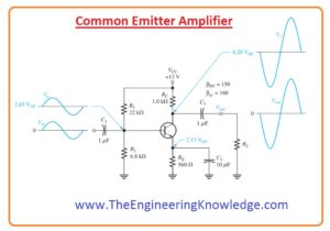
- In below figure the circuit of common emitter amplifier with the voltage bias configuration and two coupling capacitor C1 and C2 is coupled at input and output.
- There is a bypass capacitor C2 is connected from emitter to ground.
- The input voltage signal Vin is connected to the base through the capacitor and the output signal is linked to load through the collector terminal.
- The output of this circuitry is at a one-eighty degree out of phase to the input signal.
- You can note that ac voltage is provided at the base as input and output is taken at collector while the emitter is common for both input and output terminals.
- The signal at the emitter is not exiting since the bypass capacitor shorted the emitter with the ground at the signal frequency.
Phase Inversion
- The output voltage signal is not in phase with the input signal and 180 degrees out of phase. With the variation in the value of input, it varies the base ac current which causes the variation in the collector current from its Q-point value.
- With the increment in base current collector current increases above its Q-point that results in an increment in the loss of voltage about the resistance RC.
- It increases the voltage about the RC it means the voltage at collector reduces from its Q-point.
- Therefore, any variation in input signal causes an opposite change in collector signal voltage that is phase inversion.
DC Analysis
- For analyzation of above-given circuitry dc biasing firstly should be determined.
- For this dc equivalent circuitry is created by separating the coupling capacitor and bypass capacitor since they used for dc biasing.
- It also reduces the load resistance and voltage source. The resultant dc circuitry is shown in below figure.
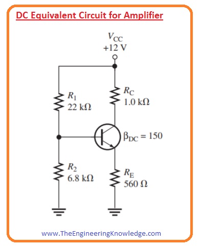
- Applying Thevenin theorem and then KVL to the base-emitter circuitry we have.
RTH=R1R2/R1 + R2
=(6.8 kΩ)(22 kΩ)/ (6.8kΩ + 22kΩ)
=5.19 kΩ
VTH=(R2/R1 + R2) VCC
[6.8 kΩ/(6.8 kΩ + 22 kΩ)]
=2.83 V
IE=VTH – VBE/RE + (RTH/bDC)
=(2.83 V – 0.7 V)/ (560Ω + 34.6Ω) =2 V
VB = VE+0.7V = 2.7V
VC = VCC – ICRC
= 12 V – (3.58 mA)(1.0 kΩ) = 8.42 V
VCE = VC – VE = 8.42 V – 2 V = 6.42 V
AC Analysis
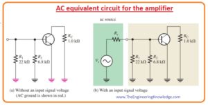
- For analyzation of ac signal operation of amplifier resultant ac circuitry can created by following steps.
- The capacitors C1, C2 and C3 can be substituted with the short circuit since their values are such that Xc is ignorable at a signal frequency and can be taken as zero ohms.
- The dc voltage source should be substituted with the ground.
- The inner resistance of dc voltage source is zero ohms since it holds a constant voltage and does not depend on the load. There is no ac voltage exits across it so it looks as an ac short. Due to this reason, the dc source is known as ac ground.
- In ac analysis of common emitter amplifier the ac ground and actual ground work as connected electrically at the same point.
- The circuit shown in the first figure called common emitter amplifier since the bypass capacitor C2 retains the emitter at ac ground.
Signal (AC) Voltage at Base
- The ac voltage source Vs is attached with the input shown in above figure denoted as (b).
- If the inner resistance of ac source is zero ohm all voltage will be shown across the base terminal.
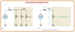
- If the inner resistance is not zero then there are 3 factors that will be taken into account for the measurement of actual value of voltage at base.
- First one is source resistance Rs, second is bias resistance R1││R2 and third is ac input resistance at base terminal of transistor Rin(base).
- It is explained in below figure denoted as (a) and simplified by connecting resistances R1, R2 and Rin(base) in parallel to obtain total resistance or Rin(tot) that is a resistance which can be seen by the ac source attached to input as denoted as (b).
- The large value of input resistance is necessary so that the amplifier will not highly load the voltage source.
- This is reverse to the conditions for a stable Q-point, that requires less value of resistances.
- The contradictory prerequisite for large input resistance and stable biasing is then one of the numerous trade-offs which should be taken when selecting apparatuses for a circuit.
- The total input resistance can be defined by this given below formula.
Rin(tot)= R1││R2││Rin(base)
- You can see in the above figure that signal source Vs, is divided between source resistance and Rs and Rin(tot) due to this the value of signal source can be calculated at base or transistor with the use of voltage divider formulas as written below.
Vb=[Rin(tot)/ (Rs + Rin(tot))]Vs
- If Rs<<Rin(tot) then Vb=Vs here Vb is input voltage to amplifier.
Input Resistance at the Base
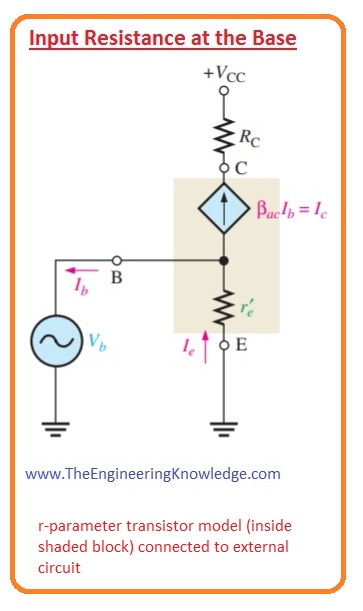
- To make an equation for the ac input resistance observing in at the base, use the basic r-parameter model of the transistor.
- In below figure the transistor model attached with the exterior collector resistance RC.
- The value of input resistance at base is given as.
Rin(base)= Vin/ Iin= Vb/ Ib
Vb= Ie r’e
As Ie=Ic
Ib= Ie/ βac
Putting values of Vb and Ib
Rin(base)= Vb/ Ib= Ier’e/Ieβac
- So we have
Rin(base)= βacr’e
Output Resistance
- The output resistance for common emitter amplifier is the resistance at the collector and is almost equal to the collector resistance.
Rout =RC
- In Rout=RC││r’c , but as the interior ac collector resistance of transistor r’c is larger than the RC the estimate is usually valid.
Voltage Gain
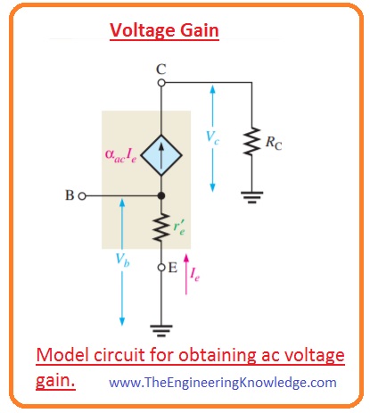
- The ac voltage gain equation for common emitter amplifier can be created with the use of model circuit as shown in below figure.
- The gain is the ratio among the ac voltage at collector Vc to the input voltage at base Vb.
Av= Vout/ Vin= Vc/ Vb
- You can see in the figure that Vc = αacIeRC= IeRC and Vb = Ier’e. so
Av= IeRC/ Ier’e
Av= RC/ r’e—-(A)
- Equation A is the voltage gain from base to collector.
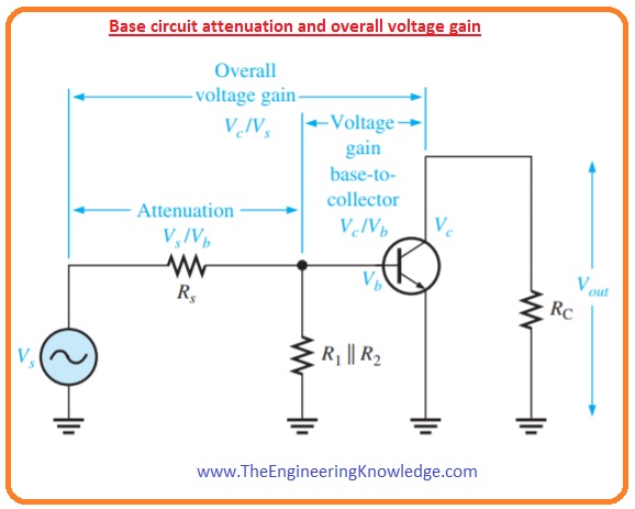
- To obtain an overall gain of the amplifier from the voltage source to the collector the attenuation of input circuitry should be added.
- Attenuation is the decrease in signal voltage as it moves through circuitry and corresponds the gain value less than one.
- For instance, if the amplitude of the signal is half the attenuation will be 2 that can be denoted as the gain of 0.5 since the gain is the reciprocal of attenuation.
- Let’s assume that a source generates a ten millivolts input signal and source resistance combined with the load resistance causes two millivolts output signals.
- In this condition attenuation is 10mv/2mV= 5.
- It means an input signal decreases the factor of five volts.
- It can be defined in terms of gain as 1/5=0.2.
- Let’s suppose that the amplifier shown in the below figure has a value of base to collector Av and the value of attenuation from the source to the base is given as Vs/Vb.
- This attenuation is generated by the resistance of the source and total input resistance of amplifier operating as voltage divider can be defined as.
Attenuation= Vs/ Vb
= [Rs + Rin(tot)]/ Rin(tot)
- The complete voltage gain of the amplifier A’v is the value of voltage gain from base to collector VC/Vb times the inverse of the attenuation Vb/Vs.
A’v= (Vc/ Vb)(Vb/Vs)=Vc/Vs
Effect of the Emitter Bypass Capacitor on Voltage
- The emitter bias capacitor that is C2 is shown in the first figure gives a short circuit to the ac signal about the resistance of emitter which keeps the emitter at ac ground which we discussed above.
- With the bypass capacitor, the gain value of the amplifier is extreme and equals to the RC/r’e.
- The value of the bypass capacitor should be high enough so that its reactance over the frequency range of the amplifier is very (almost zero) less than the RE.
- The simple rule is that capacitance reactance XC of bypass capacitor must be at least ten times less than RE at less frequency should function.
- 10XC less than or equals to RE
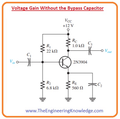
Voltage Gain Without the Bypass Capacitor
- To observe the effect of bypass capacitor on ac voltage gain let us eliminate it from the circuitry and compare the voltage gain as shown below figure.
- In the absence of a bypass, the capacitor emitter will not remain at ac ground.
- Instead, RE is seen by the ac signal between the emitter and ground and efficiently adds r’e to the voltage gain formula.
Av= RC/ (r’e+ RE)
- The fact of RE is to reduce the ac voltage gain.
Effect of a Load on the Voltage Gain
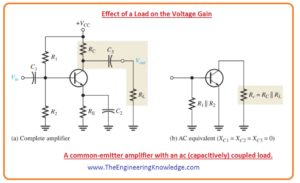
- The amount of current use by the output of transistor or any circuity through the load resistor when the resistance RL is attached to the output through the coupling capacitor C3 it shown in the below figure denoted as (a).
- The collector resistance at the signal frequency is RC connected in parallel with the load resistance RL.
- Recall, that the upper end of RC is at ac ground. The ac corresponding circuity is denoted as b in the below figure.
- The total ac collector resistance will be.
Rc=RCRL/(RC + RL)
- Substituting RC in place of Rc in the equation of voltage gain we have.
Av=RC/r’e
- When Rc<RC due to resistance RL, the voltage gain is decreased. Though, if RL>>RC then Rc=RC load has very less effect on the gain.
Stability of the Voltage Gain
- Stability is a measurement of how much good an amplifier retains its design values when there is variation in temperature or in case of the different transistors with different β.
- Though bypass resistance Re does not generate the highest value of voltage gain there are issues of stability as the ac voltage gain depends on the r’e as AV=RC/r’e.
- Stability is a measurement of how much good an amplifier retains its design values when there is variation in temperature or in the case of a different transistor with different β.
- Though bypass resistance Re does not generate the highest value of voltage gain there are issues of stability as the ac voltage gain depends on the r’e as AV=RC/r’e.
- Though with the resistance RE is unbypassed the gain less depend on the r’e.
- If RE>>r’e the gain does not depend necessarily on the r’e since.
Av=RC/RE
Swamping r’e to stabilize the voltage gain
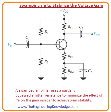
- Swamping is a process used to reduce the effect of r’e without decreasing the voltage to its minimum value.
- Swamping in fact is a compromise among having a bypass capacitor and does not have a bypass capacitor.
- In swamped amplifier resistance RE is partially bypassed so that enough gain be obtained and the effect of r’e is completely decreased or minimized.
- The total exterior resistance RE is created with 2 separate emitter resistance RE1 and RE2 as shown in the below figure.
- One resistance RE2 is bypassed and second is not.
- Both resistances (RE1+RE2) affect the dc bias but RE1effect the ac voltage.
AV=RC/(r’e+RE1)
- If RE1 is 10 times greater than the r’e then the effect of r’e is reduced and the approximated value of voltage gain is.
Av=RC/RE1
Effect of swamping on Amplifier’s Input resistance
- The ac input resistor observing at the base of common emitter amplifier with RE totally bypassed will be Rin=Bacr’e
- When emitter resistance has partly bypassed the part of resistance that is not bypassed can look through the AC voltage signal that causes in the increment in ac input resistance by connecting in series with r’e. the resultant equation is Rin(base)=βAC(r’e+RE1).
Current gain
- The equation of current from base to collector is Ic/Ib or βAC.
- As an overall current gain of common emitter amplifier is.
- Ai=IC/Is
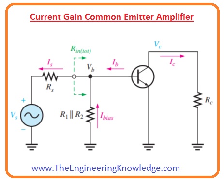
- It is the total signal input generated by the source its first portion is Ib flowing through the base and second is Ibias passes through the bias circuit (R1ІІR2) as shown in below circuit.
- The source sees a total resistance of Rs+Rin(tot).
- The total current generated by the source is given as.
Is=Vs/(Rs+Rin(tot))
Power Gain
- The power gain is the multiple of overall gain of current gain and voltage gain.
- AP=Av’/Ai
- Av’ is equal to the Vc/Vs
So, friends, it is a detailed post about common emitter amplifier if you have a question ask in comments. Thanks for reading.

